Project update 5 of 9
Manufacturing Process
Hello backers!
The USB Armory batch production is almost complete and we would like to take this opportunity to provide some details about the manufacturing process. The journey that takes the USB Armory design from schematics to the physical board is truly fascinating and involves several steps.
We decided from a very early stage to manufacture and assemble the USB Armory PCB 100% in Italy, which is where Inverse Path is based. This allows us to efficiently interact with our suppliers and ensure the quality that the USB Armory boards deserve.
The PCB manufacturing is done by TVR, a high quality "Just in Time" manufacturer founded in 1975. Their manufacturing capabilities, efficiency and process quality are remarkable, they are highly praised for the quick turnover in producing complex PCBs with an extremely low failure rate.
The board assembly is done by CIPIERRE, a company established more than 20 years ago and considered one of the best in the country within its field. Their involvement has been essential not only to ensure a smooth manufacturing, but also to provide efficient procurement of all the USB Armory components at the lowest possible cost for our batch size.
Let us breakdown the various phases involved in producing the USB Armory at our specific manufacturers.
Computer Aided Manufacturing (CAM)
The USB Armory schematic and PCB layout has been entirely developed by Inverse Path using the Open Source KiCad EDA Software Suite.
The manufacturing output of such process is the CAD data, contained in a set of files defined by various industry standard formats.
Artwork data (Gerber): defines the inner and outer layers, the soldermask, legend (silkscreen) and solder paste
Edge cuts (Gerber): defines the physical dimensions of the board
Drill map (Gerber): defines required drill points
Netlist (IPC-D-356): defines all electrical connections, used for PCB electrical testing
Stackup: defines the arrangement of the PCB layers, their individual thickness and material
The CAM department of the PCB manufacturer takes all of these inputs, adjusts them for the specific manufacturing process by defining the production panel, used for the PCB production, and the customer panel, used on the assembly line.
Inner Layer Surface Treatment
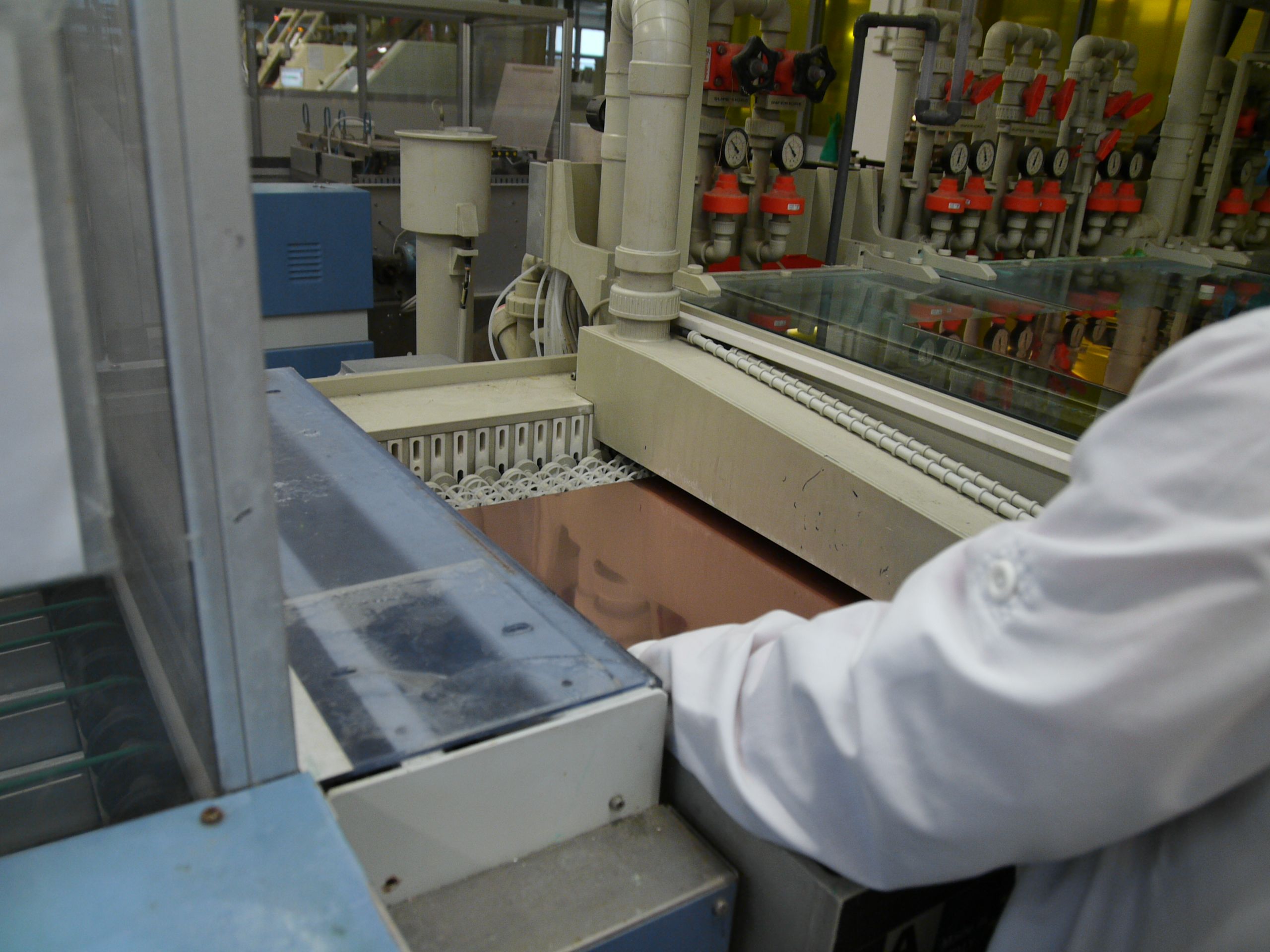
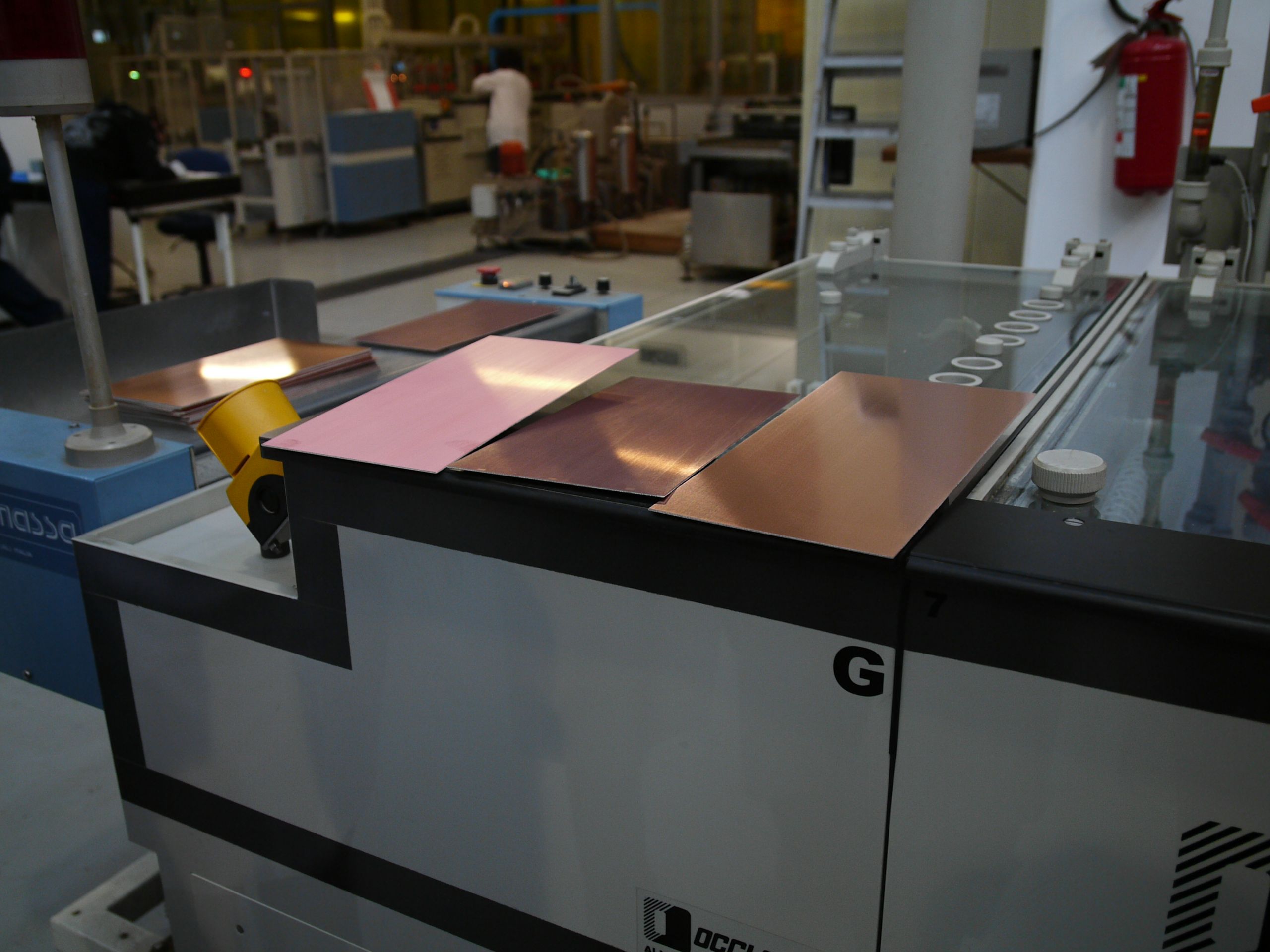
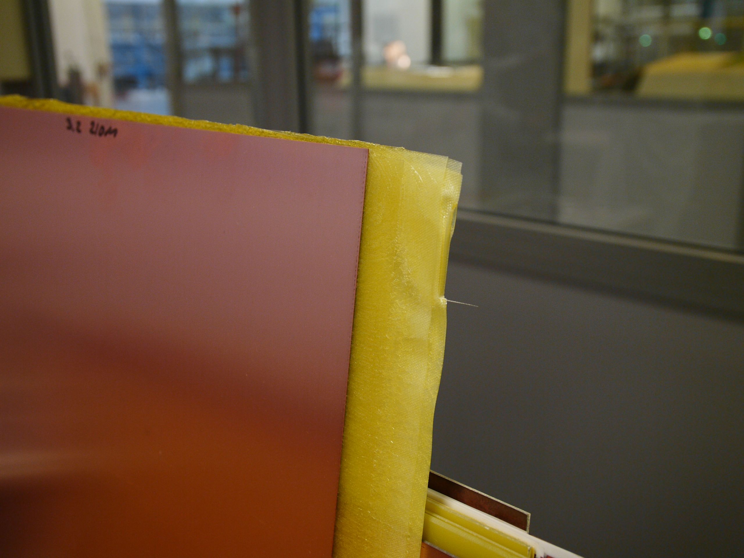
The first manufacturing steps consist of taking copper-clad laminates, compliant for the specified stackup, and surface treat them with a micro-etching solution (MECetchBOND) that prepares the copper for optimal dry film or solder mask application.
Dry Film Application
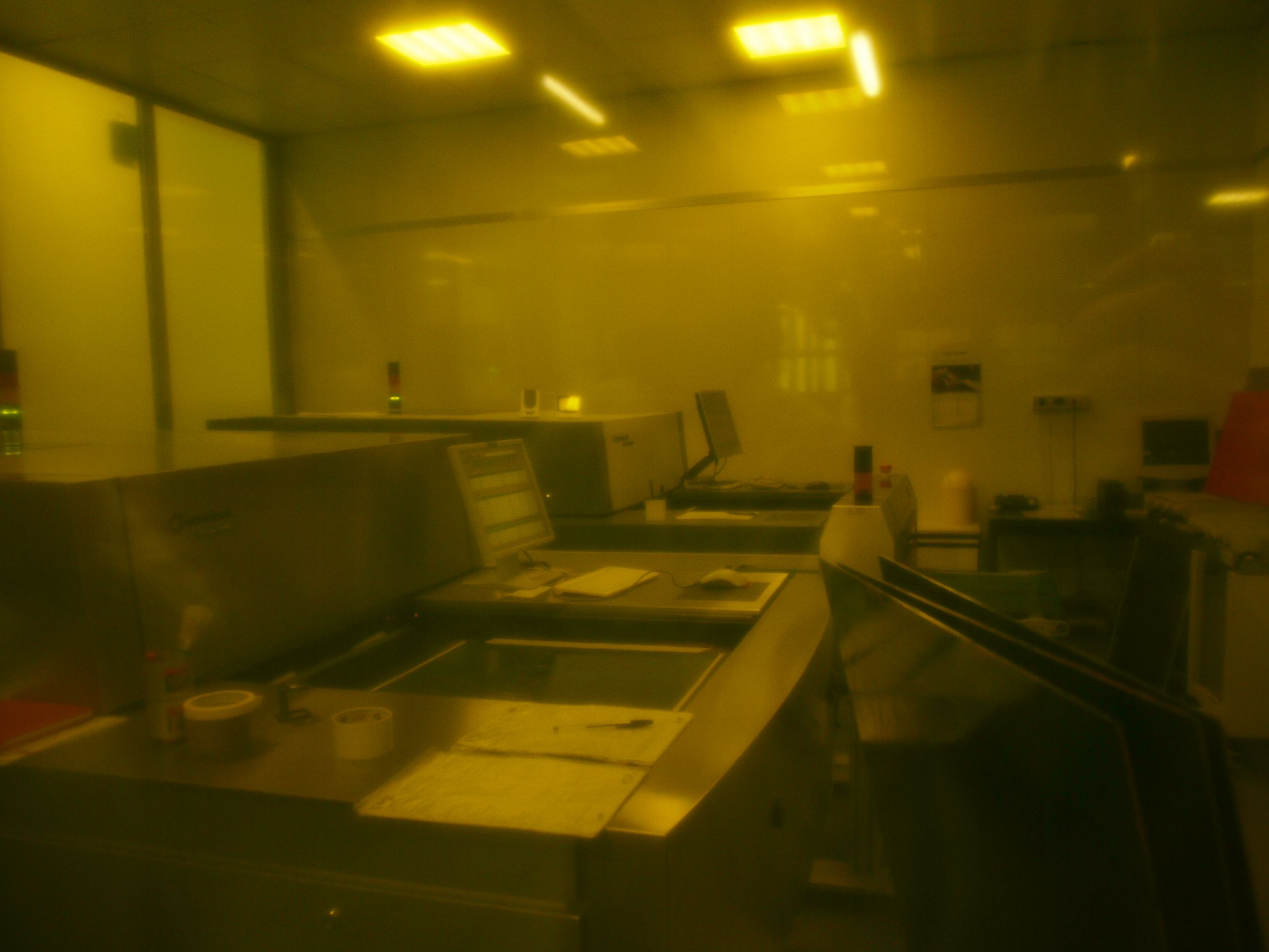
The laminates are being coated with the dry film photo-resist. This is accomplished in the so called "yellow room", as photo-resist is sensitive to UV light, with the aid of a Dow Automatic Laminator 1600-SPC/T machine
Laser Direct Imaging (LDI)
The LDI process allows to avoid traditional film creation by laser imaging the artwork directly on the dry film.
The artworks are derived from the inner layer Gerber files and printed on both sides of the copper-clad laminates. This process has a precision down to 50 microns for track width and gaps and guarantees extremely high quality.
An Orbotech Nuvogo 800 is used for this process.
Inner layer etching
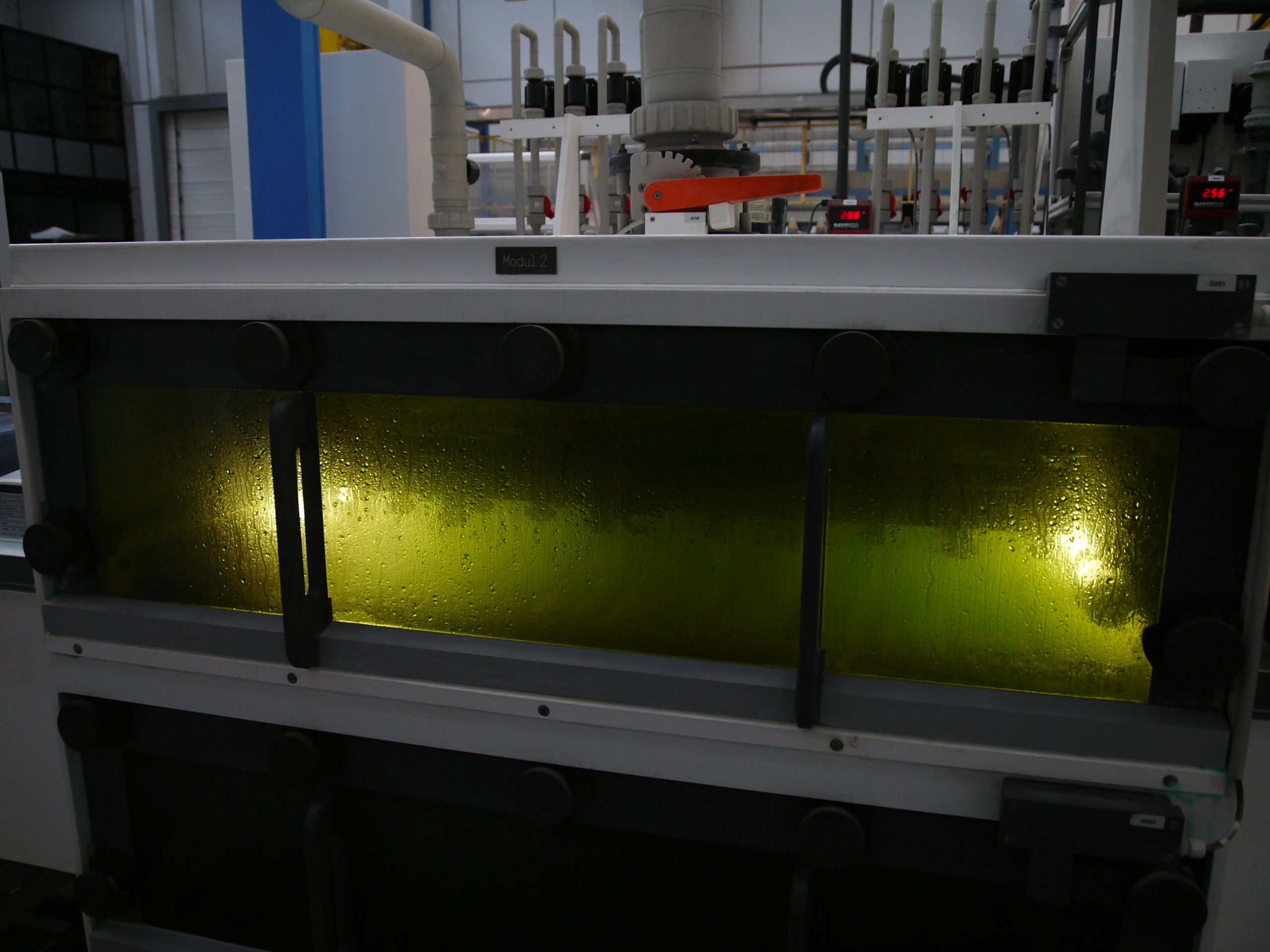
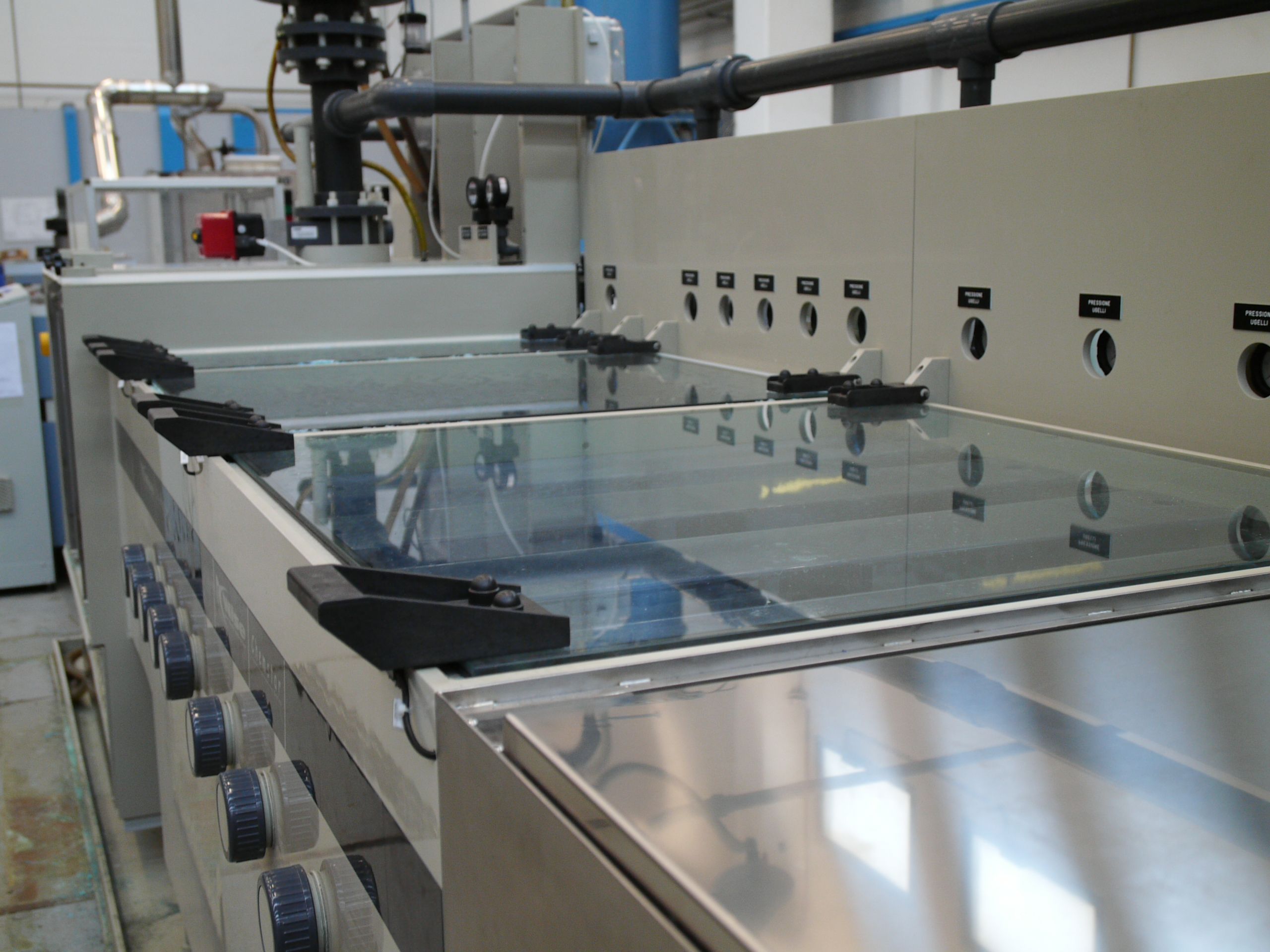
The unexposed copper is etched away using an alkaline solution. Following this, the hardened dry film still present on the exposed copper is cleaned away and the copper-clad laminate is dried.
Automated Optical Inspection (AOI)
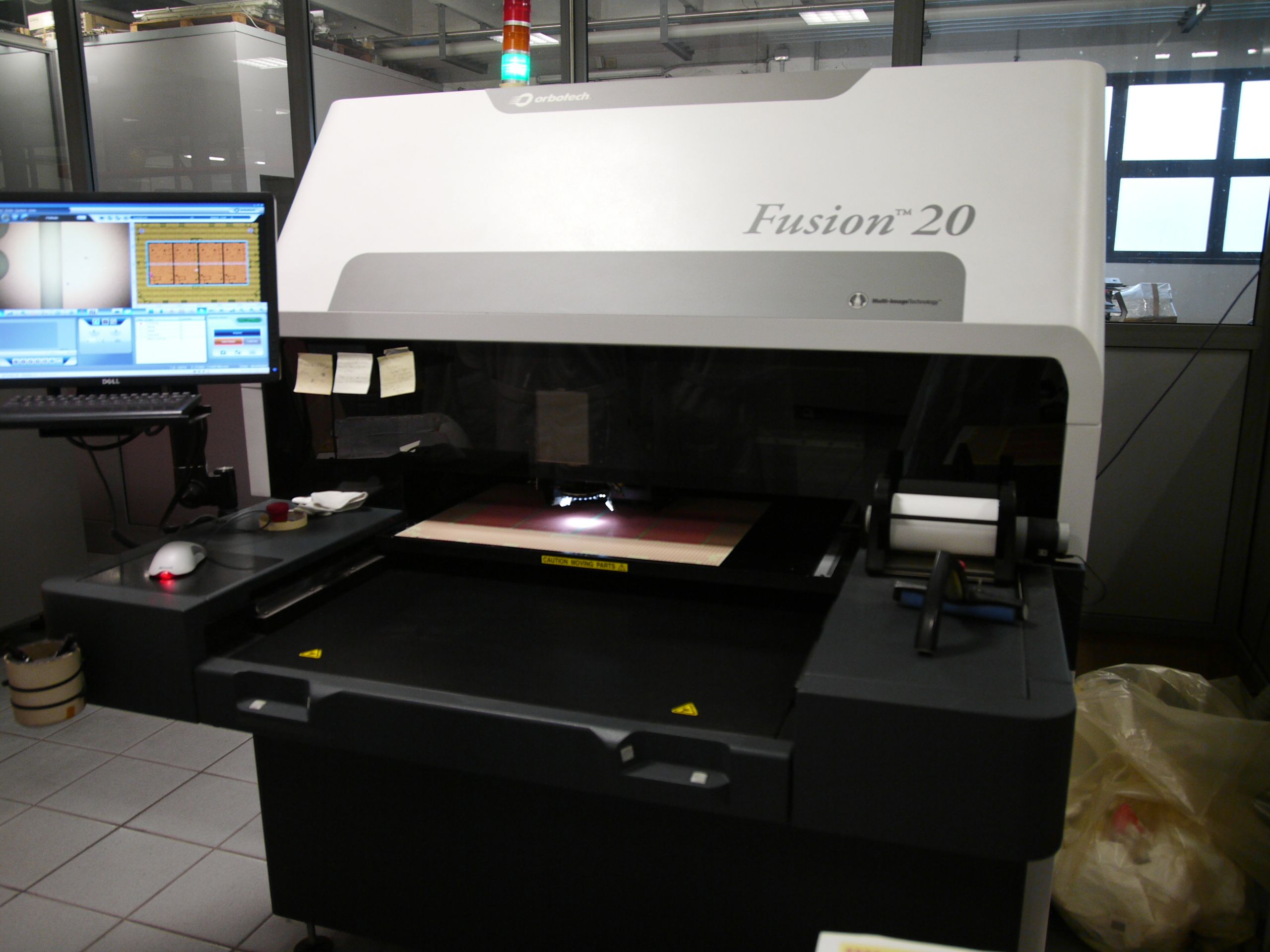
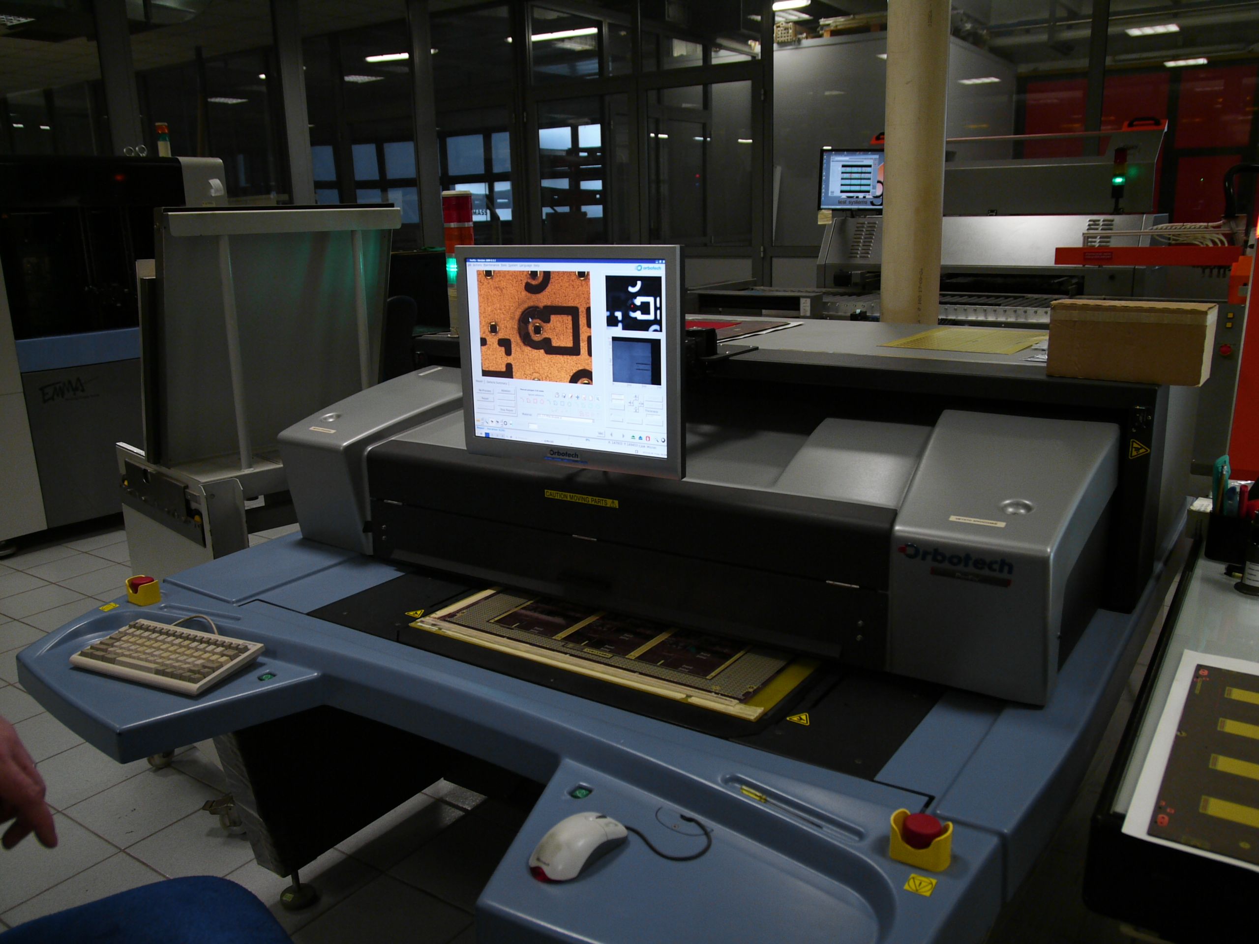
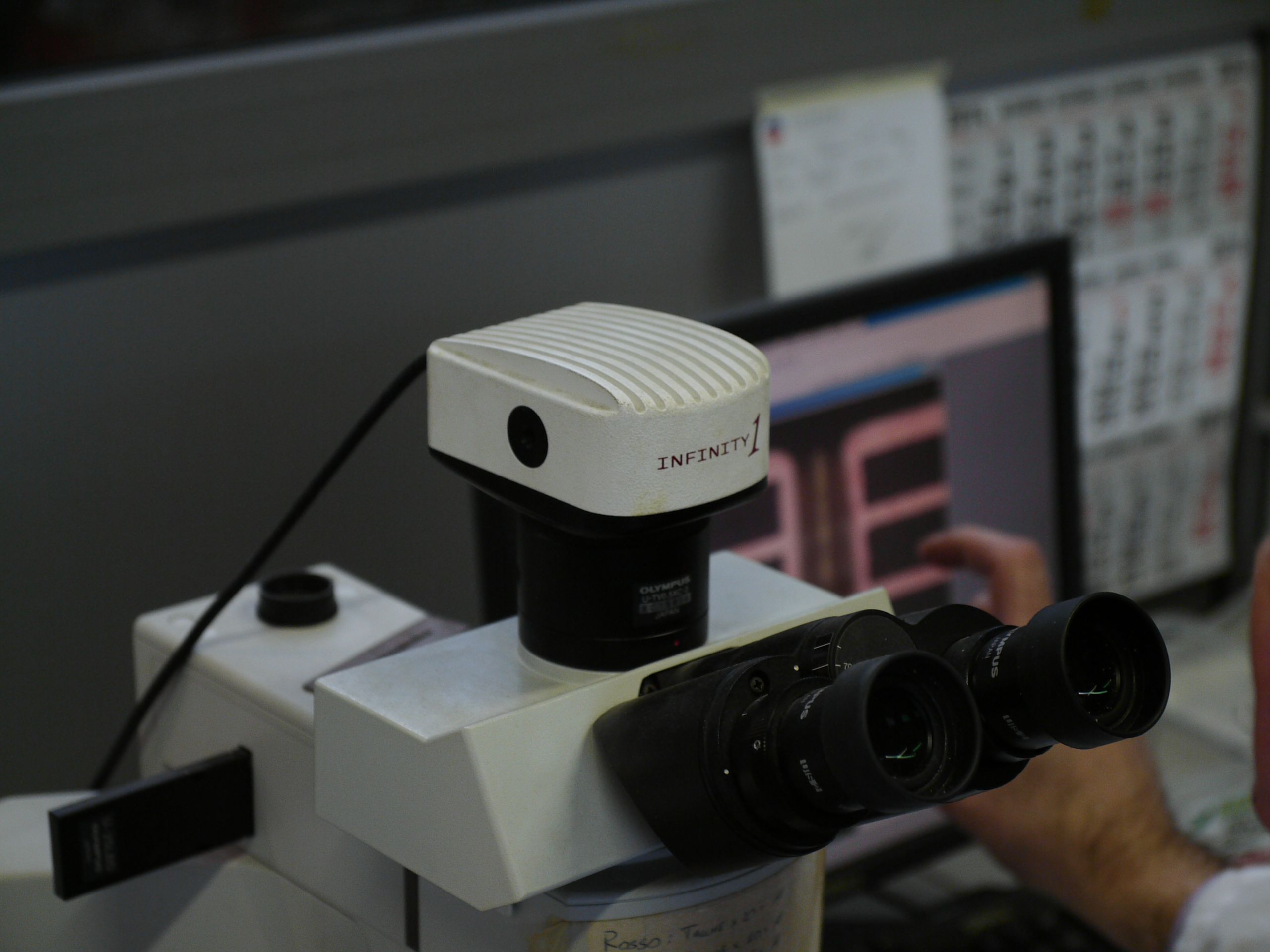
The two sides of the copper-clad laminate are compared with digital images. This is a crucial step as any imaging defect cannot be corrected afterwards. In case a flaw is found an Automated Optical Rework (AOR) machine can be used to address it.
The inner layers inspection is done with an Orbotech Fusion 20 machine.
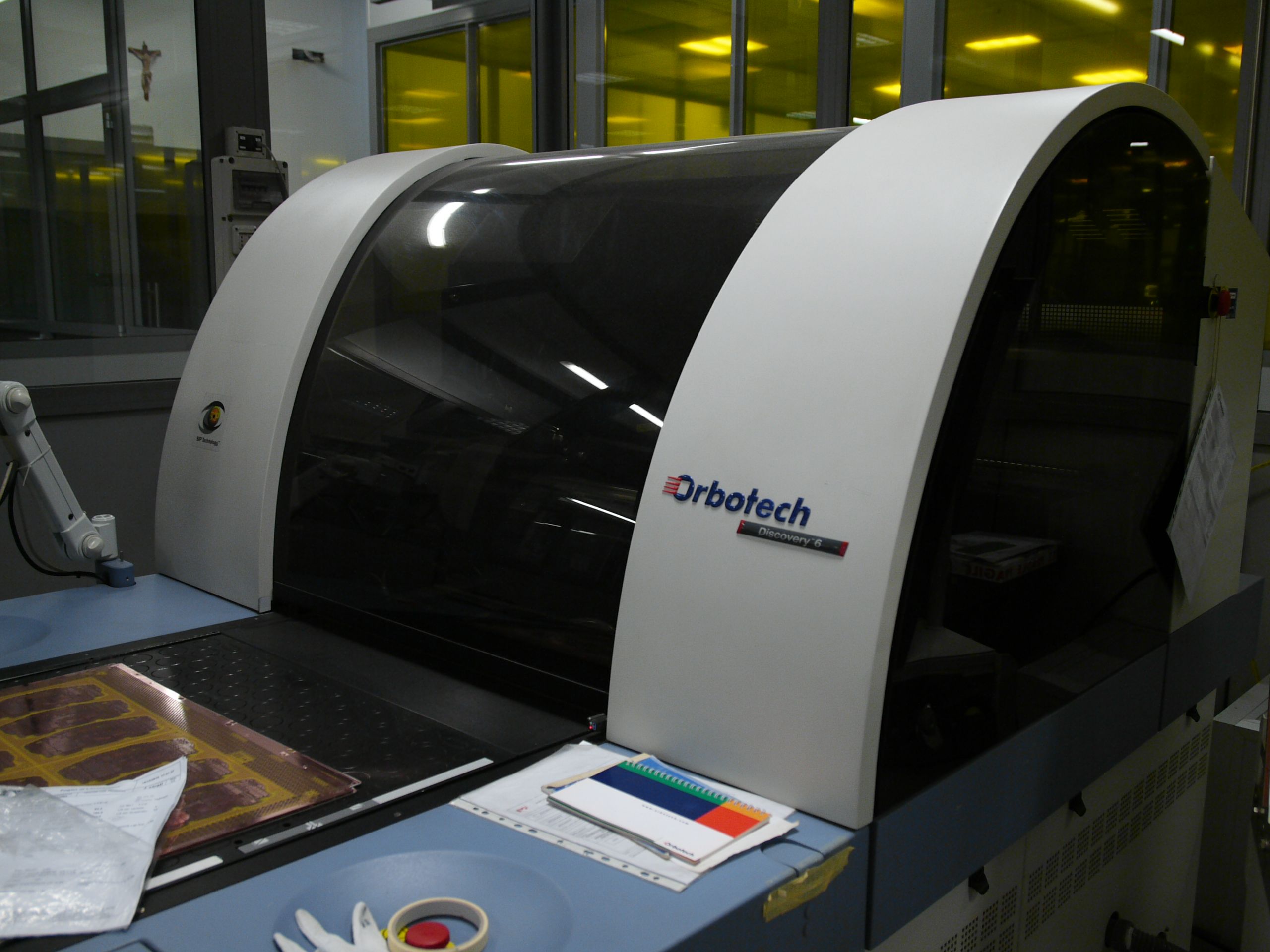
The outer layers are inspected with an Orbotech Discovery 6.
The AOR machine is an Orbotech PerFix.
The inner layers are then registered and punched, assuring correct alignment in the next phase.
Inner layer oxidation
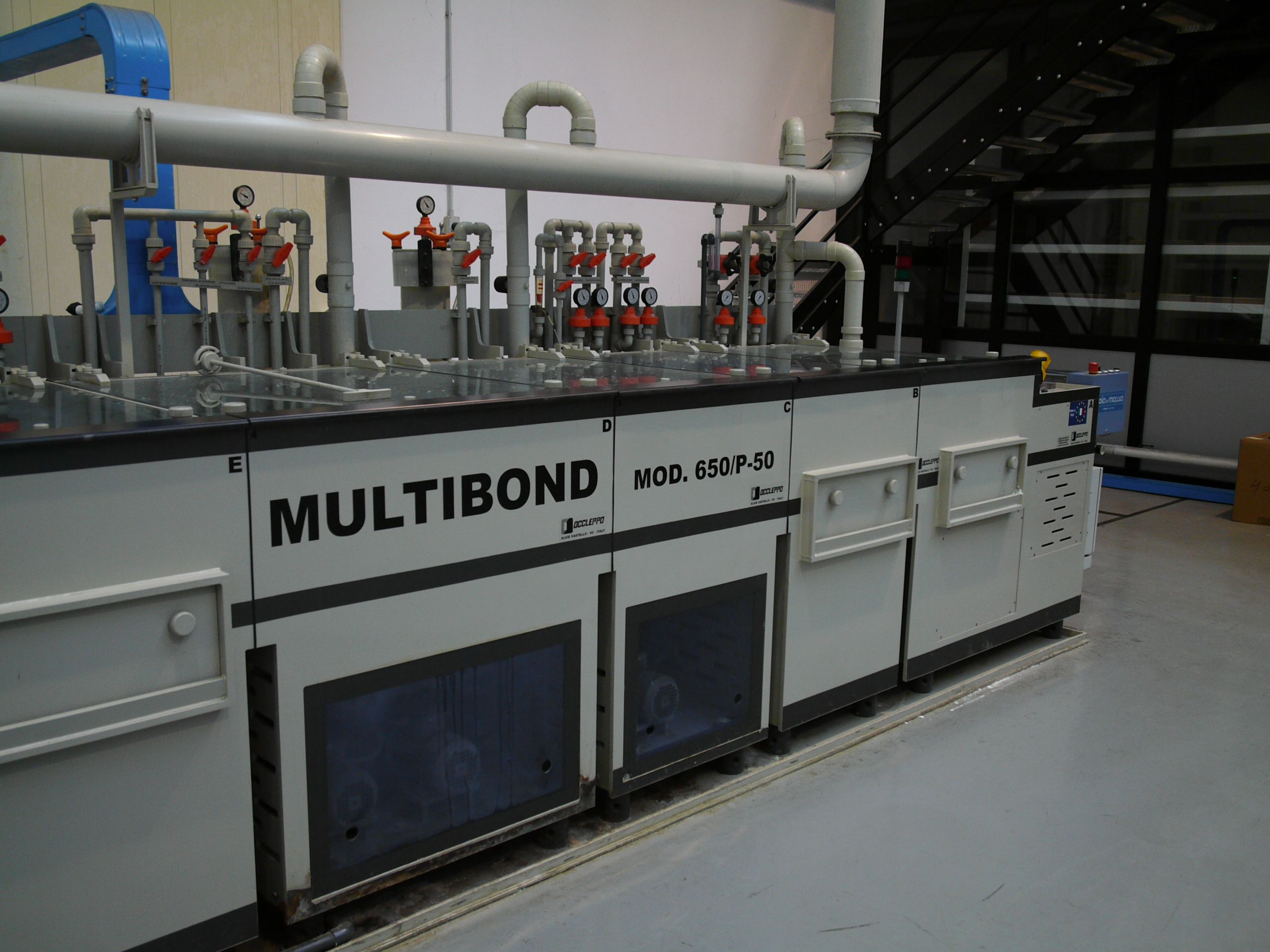
The inner layer oxidation ensures enhanced bonding between them and the prepregs (the FR4 material between two laminates). This is accomplished using a dedicated multibond machine manufactured by OCCLEPPO, an Italian company based in Turin that has been around since 1963.
Bonding
The final PCB stackup is made with the following foils (6 copper layers in total for the USB Armory):
- copper foil
- prepreg
- laminate
- prepreg
- laminate
- prepreg
- copper foil
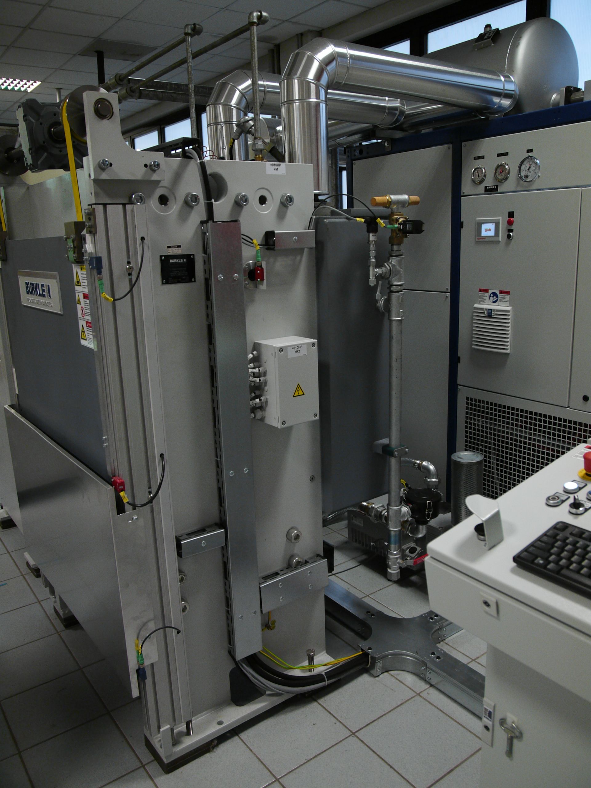
The inner layers are correctly aligned through drills made during the previous steps. The stack is inserted in the bonding machine where precise pressure and heat are applied. The epoxy resin in the prepregs melts and act as a glue between the laminates. A Bürkle multilayer press is used for the task.
X-ray Drilling
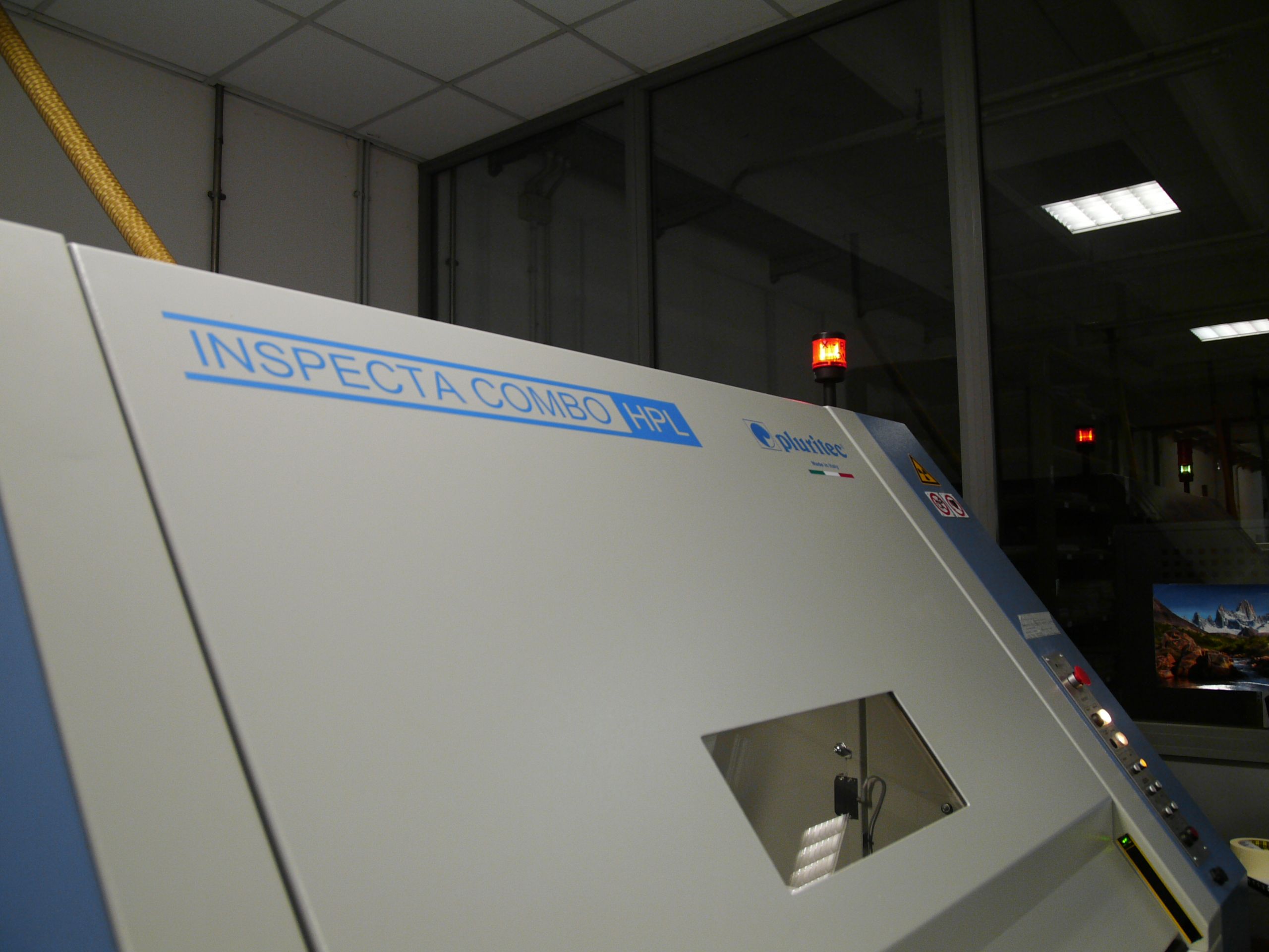
The PCB is now of the final thickness and all layers are covered by copper. To correctly align the outer layer with the inner ones, an X-ray drilling machine is used to locate targets buried in the inner layers and drill registration holes.
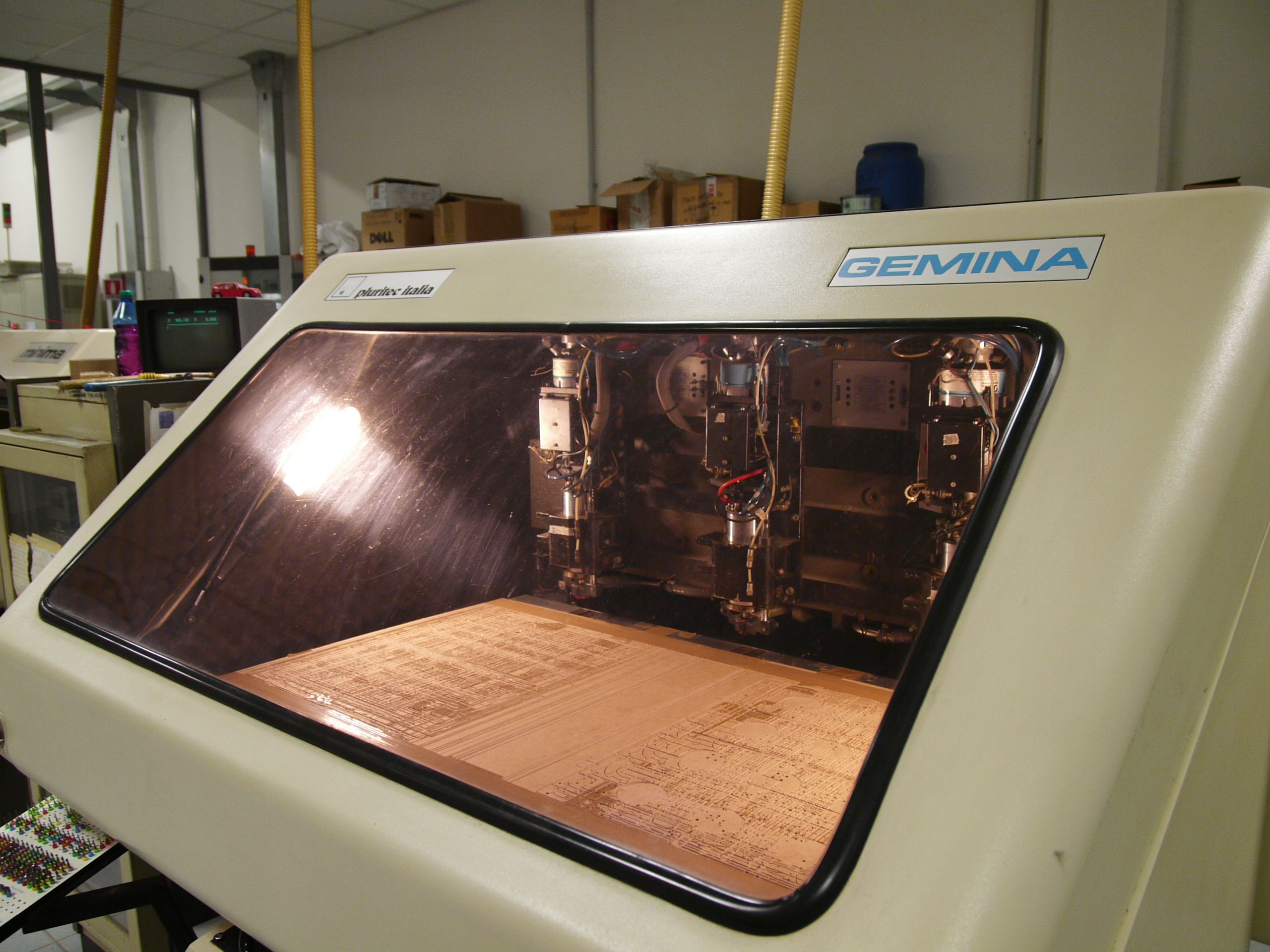
This is accomplished by another machine from an Italian manufacturer, a Pluritec Inspecta Combo HPL.
Drilling
On the bottom and upper layers a steel foil is placed to aid the drilling process. The vias are deburred and the entire PCB is cleaned from residual dust.
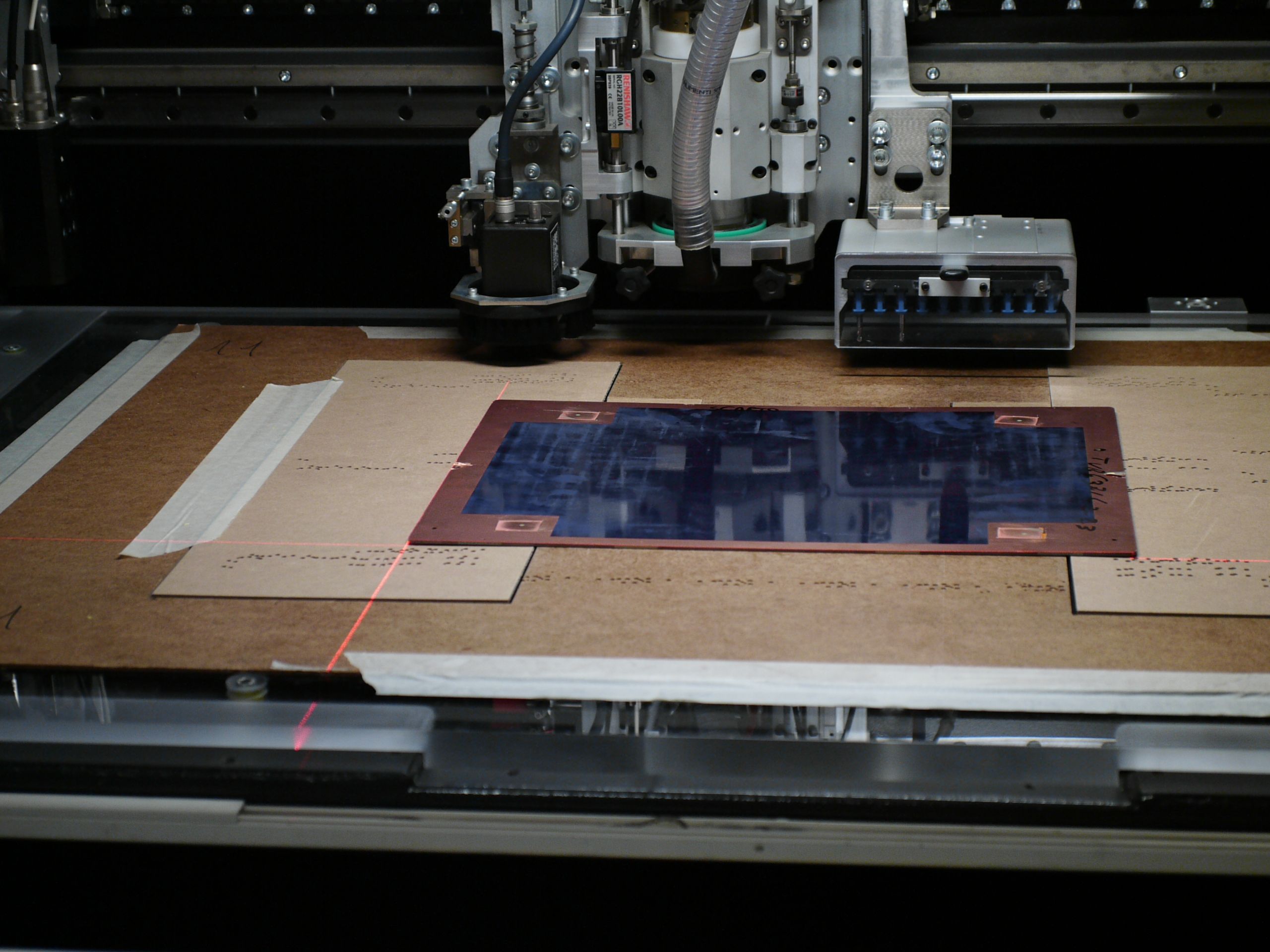
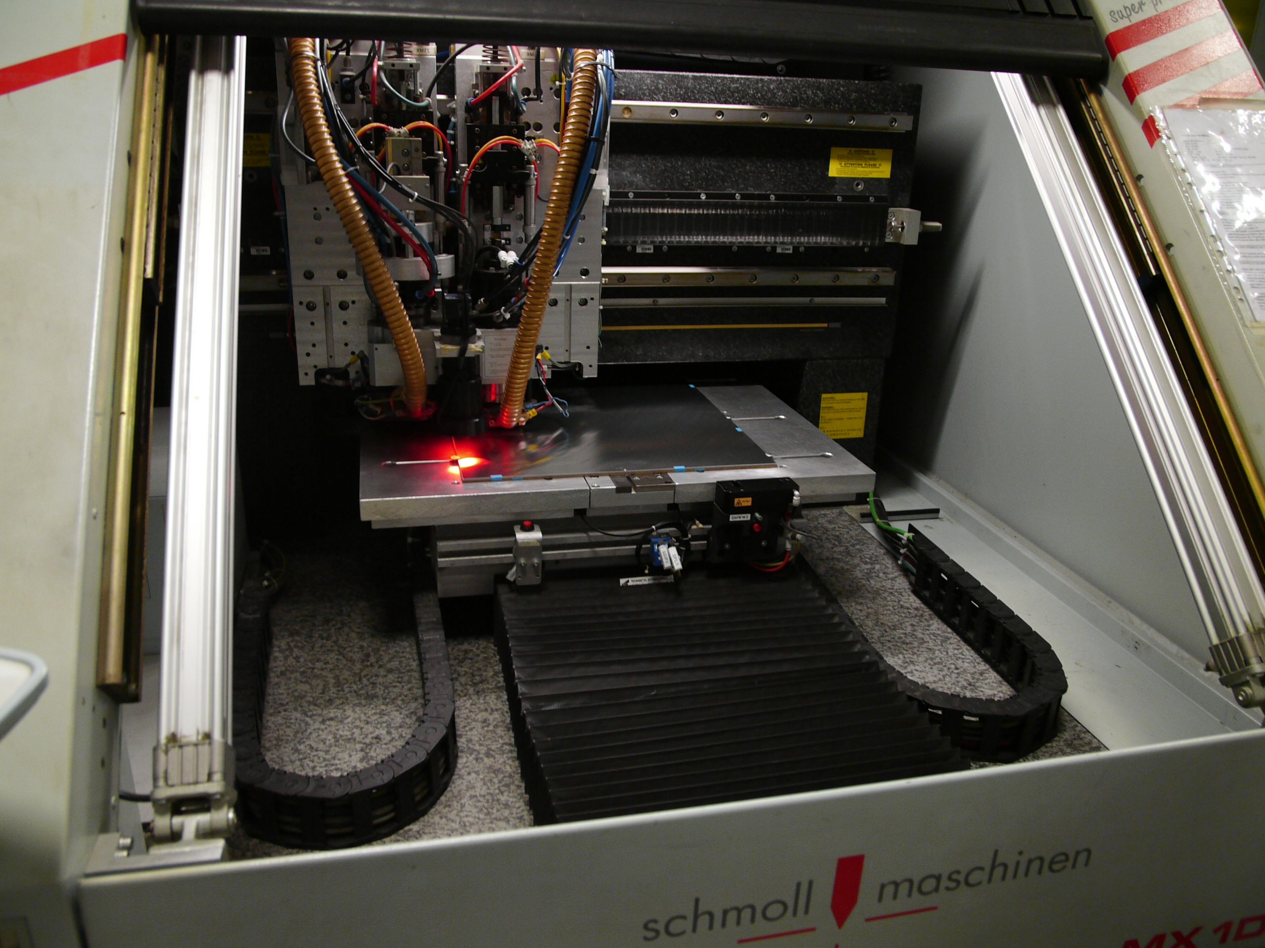
The drilling is accomplished with a Schmoll Maschinen A-MX 1DH. It is interesting to note that the average individual drill head life is only of a few thousand drills, to ensure precision. The machine therefore packs an impressive array of drill heads "ammo" to automatically dispose and reload them.
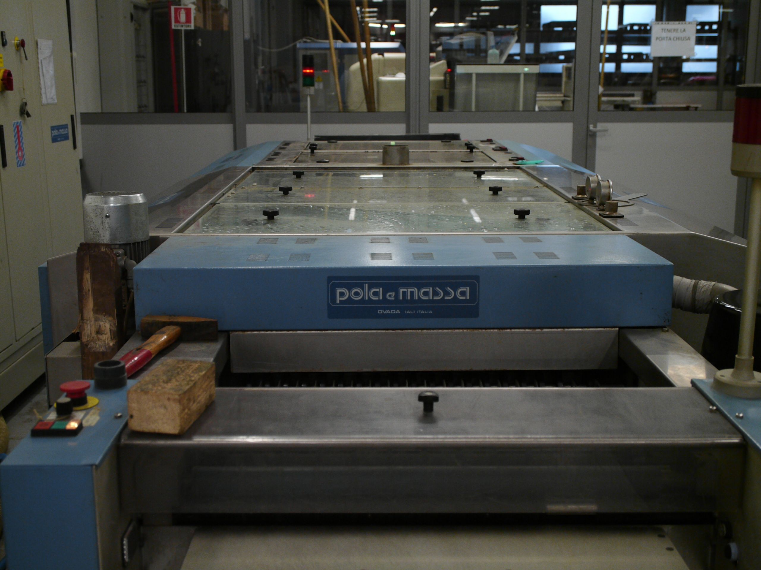
The cleaning is done with a machine from Pola e Massa, an Italian company established in 1978, leader in deburring/scrubbing machines manufacturing.
Electroless plating
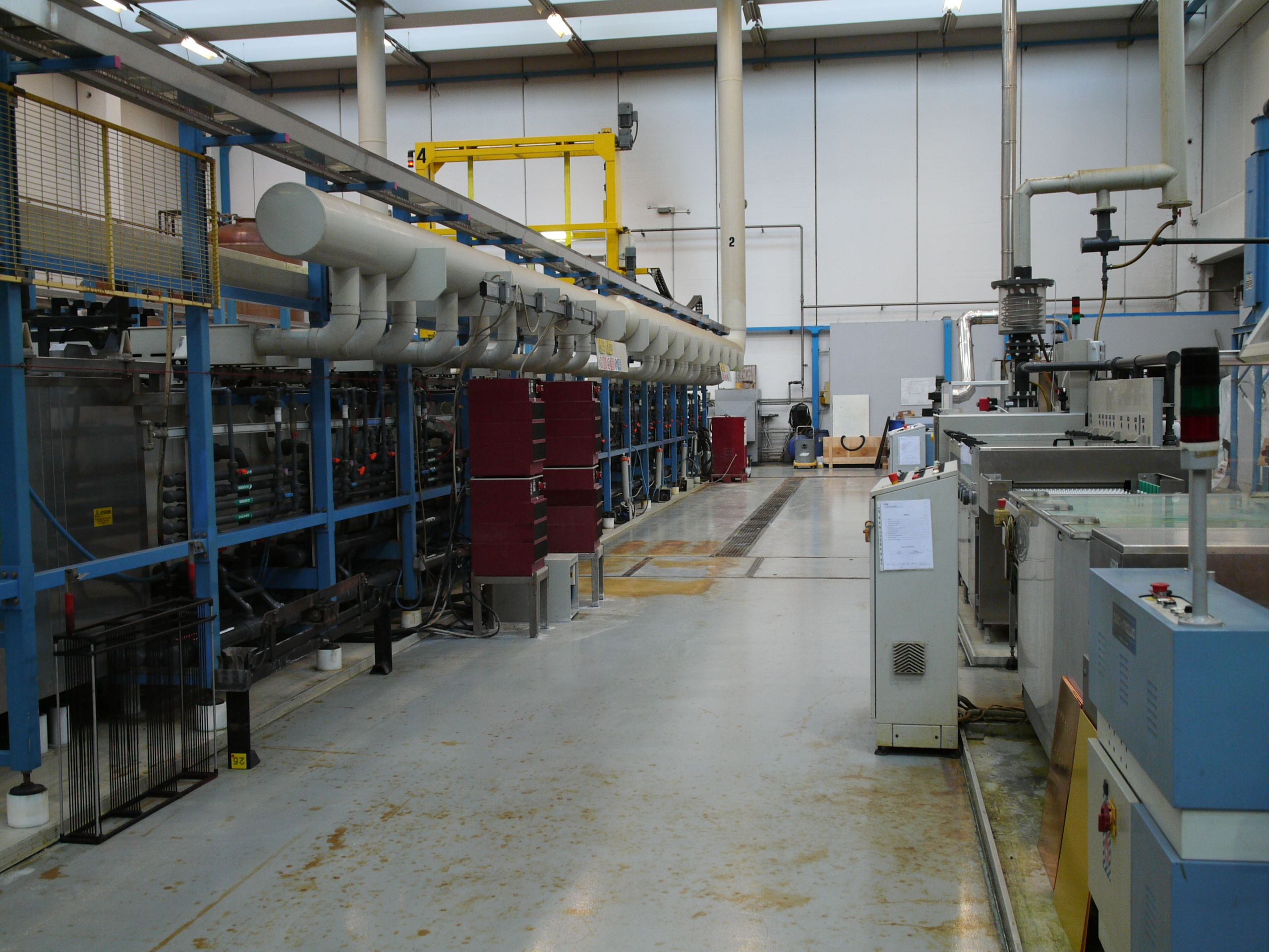
Electroless copper deposition is performed to deposit a thin (~1 micron) layer of copper.
Electroplating
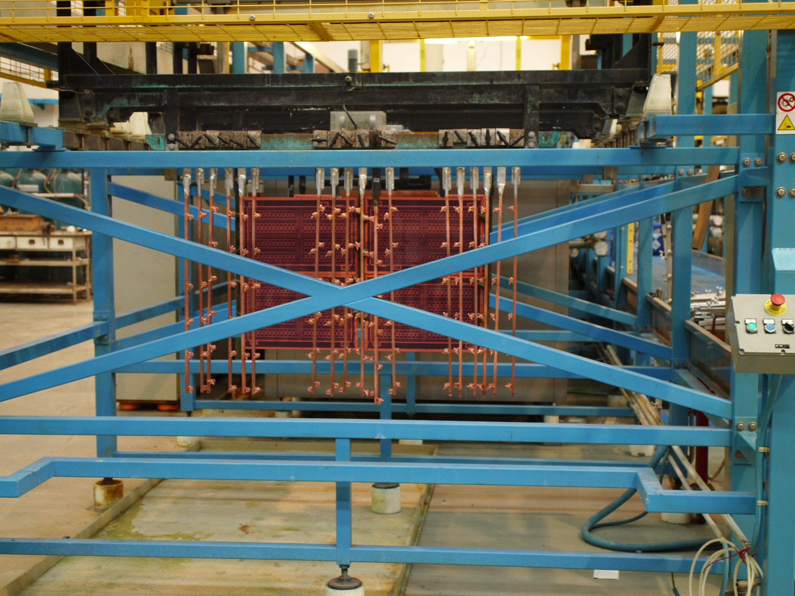
The PCB surfaces act as cathodes for the electroplating. Around 20 microns of copper is grown on the entire exposed copper, in the vias and on dry-film exposed copper.
Outer layer etching
The plated copper is now covered by tin and the Strip Etch Strip (SES) process takes place: Strip the resist to expose the unwanted copper, Etch the exposed copper, Strip the protection tin. This is done on a single assembly line.
Solder resist
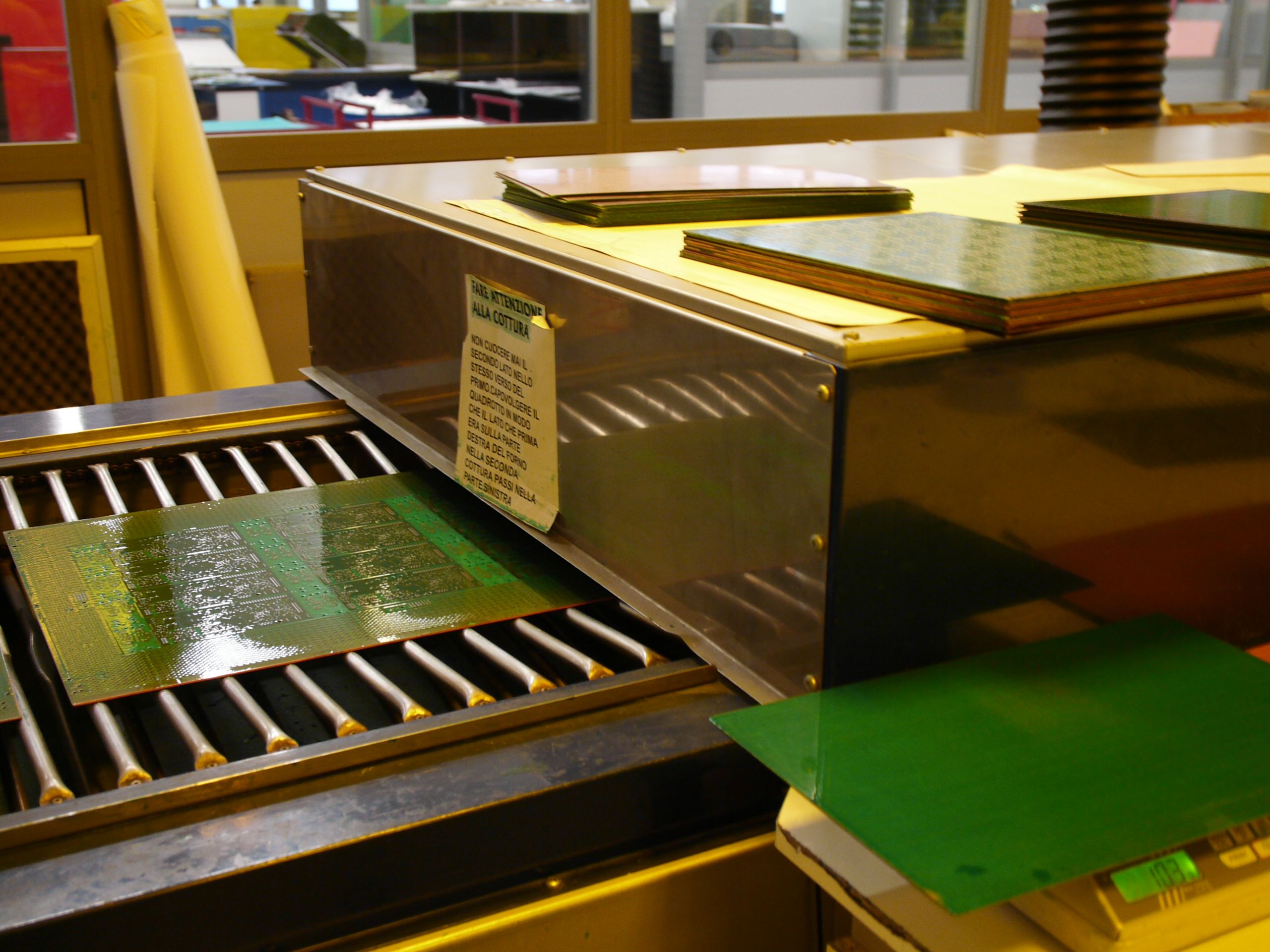
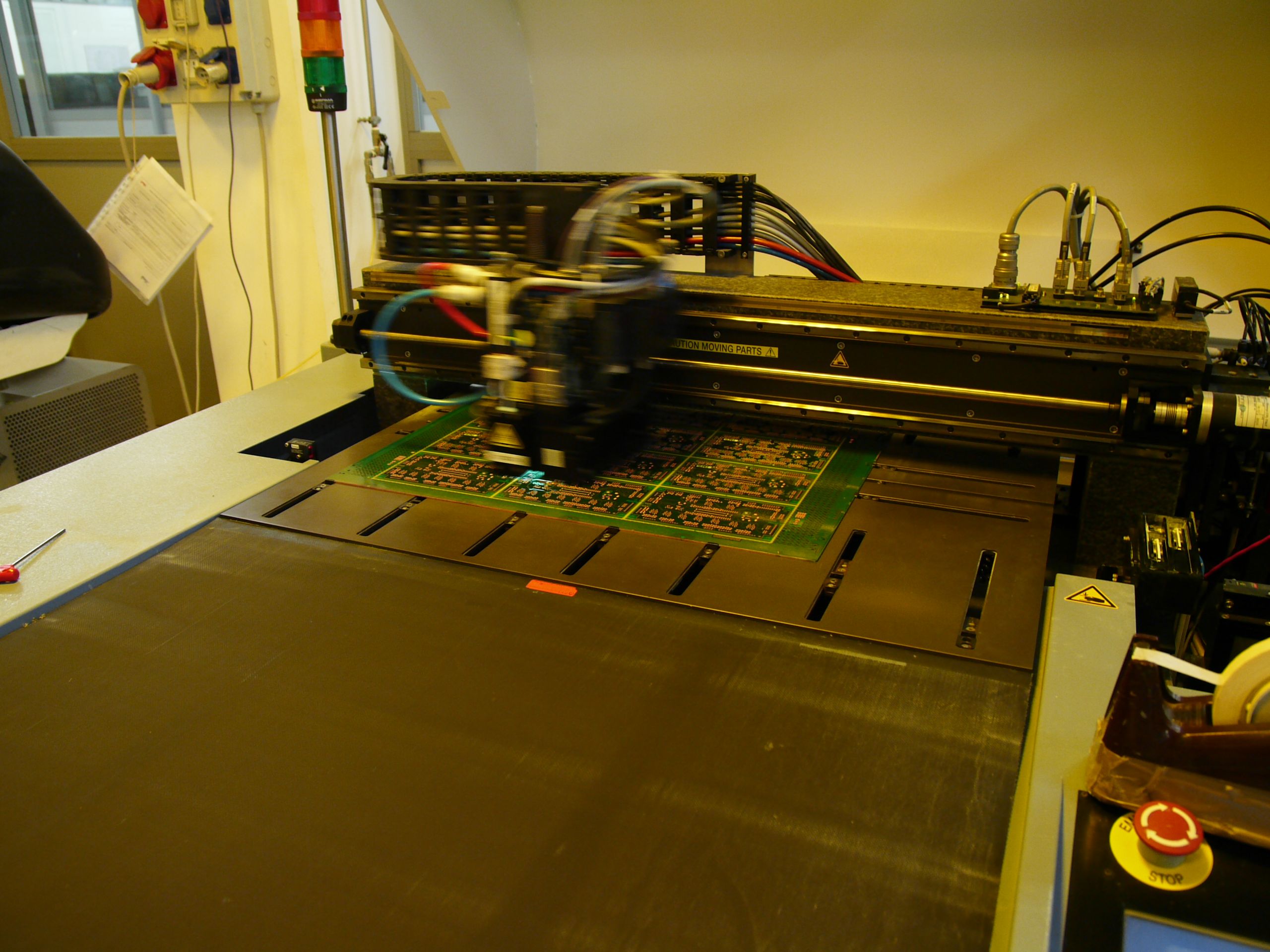
The entire PCB is now covered with a Liquid Photo Imageable (LPI) and the photoresist is printed on it. After the developing phase the soldermask is open and the copper is exposed only on soldering pads.
The purpose of the soldermask is to protect the outer layer copper from oxidation and prevents solder bridges in the component soldering phase.
In Europe the soldermask is traditionally green, however the USB Armory boards get a black solder mask treatment as this looks, in our opinion, way cooler :).
Finishing
The exposed copper pads must be protected from oxidation and prepared for being soldered. In the ENIG (Electroless Nickel Gold) finishing around 5 microns of nickel are deposited under a very thin layer of gold (~1 micron). This kind of finishing assures the planarity needed for the BGA components (SoC, RAM in our case).
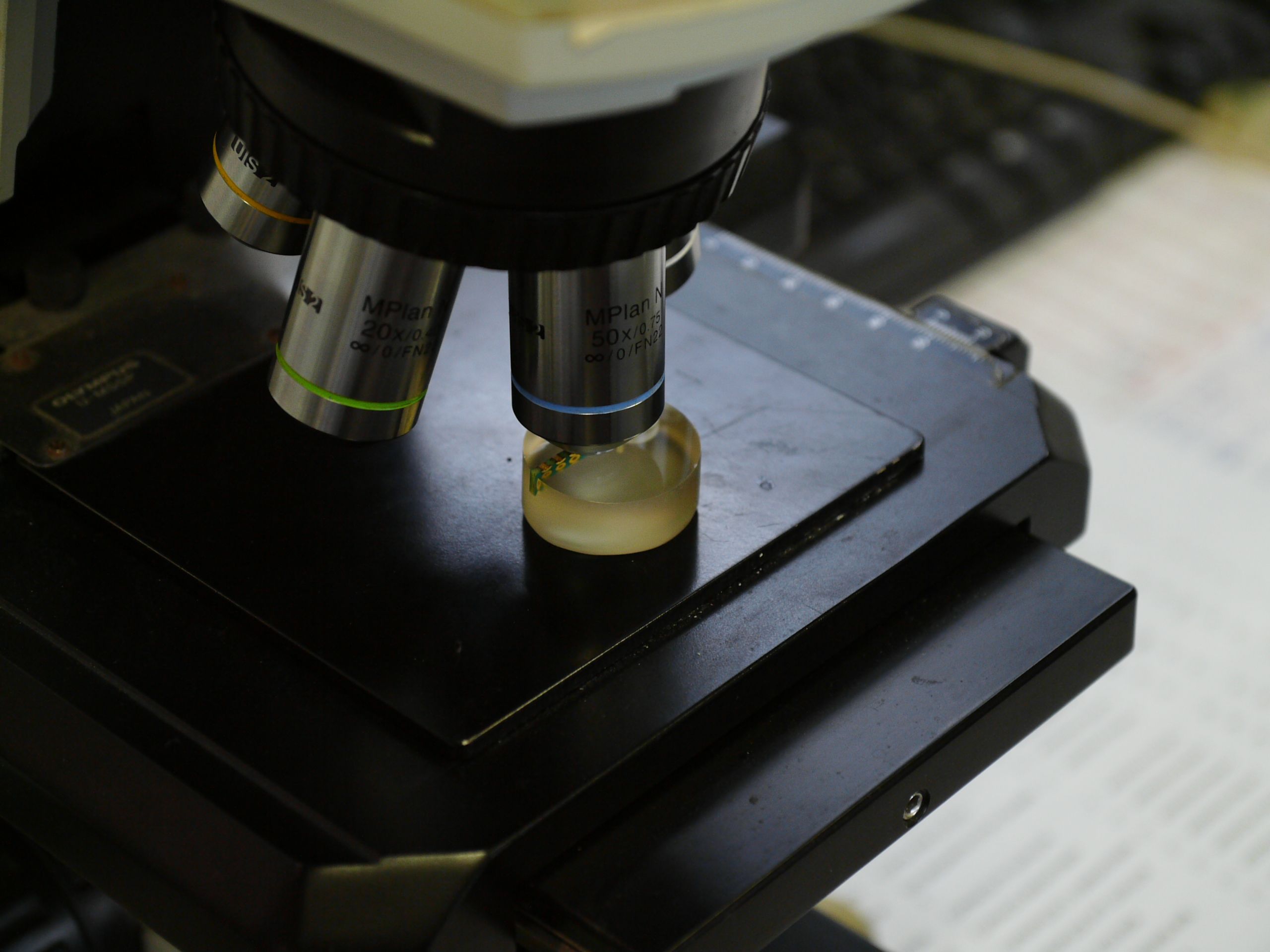
On high quality production runs a metallographic analysis is made after this stage to check the correct material growth of copper foils, plated copper, nickel and gold.
Gold Edge plating
The Electroless applied gold is excellent for soldereability, however it is too soft to cope with the repeated insertions needed for the USB connector. Therefore an additional ~2 microns of gold are selectively electroplated only on the four USB connector pads.
Silk screen
The silkscreen legend printing is performed using an inkjet PCB printer powered by UCI technology (UV Curing Integrated), the used printer is an Orbotech Sprint 8.
This technology allows to print the silkscreen with high speed and accuracy, additionally a closed loop ink supply system prevents ink waste. We were very happy to learn that the innovative technology used for this silkscreen printers was acquired by Orbotech from a local company based in Gorizia - Italy, founded by a former university colleague of the Inverse Path team.
Routing and beveling
Two levels of "routing" are performed. The "inner" routing cuts out the final component, while the "outer" routing cuts out the customer panel.
Electrical Test
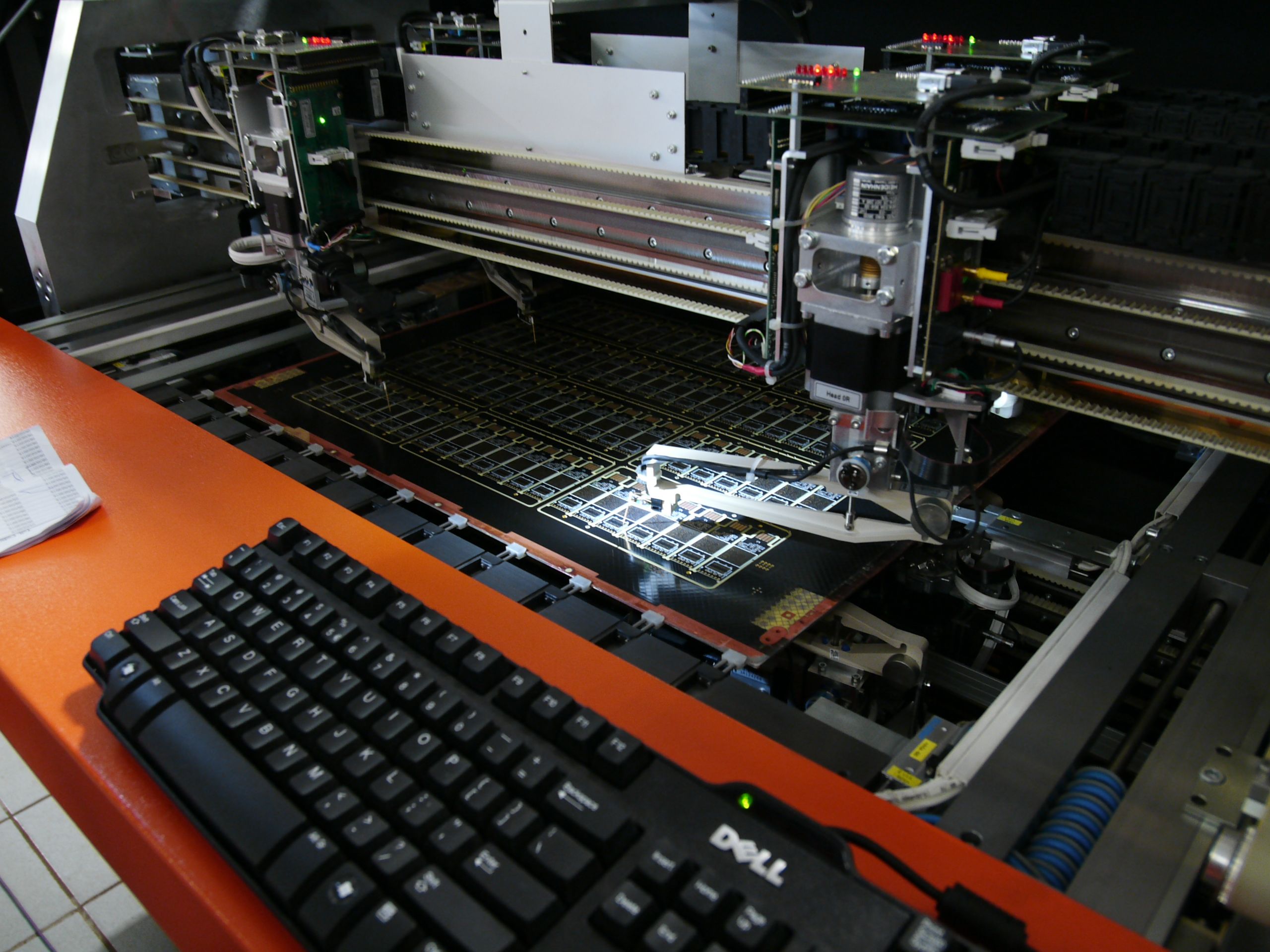
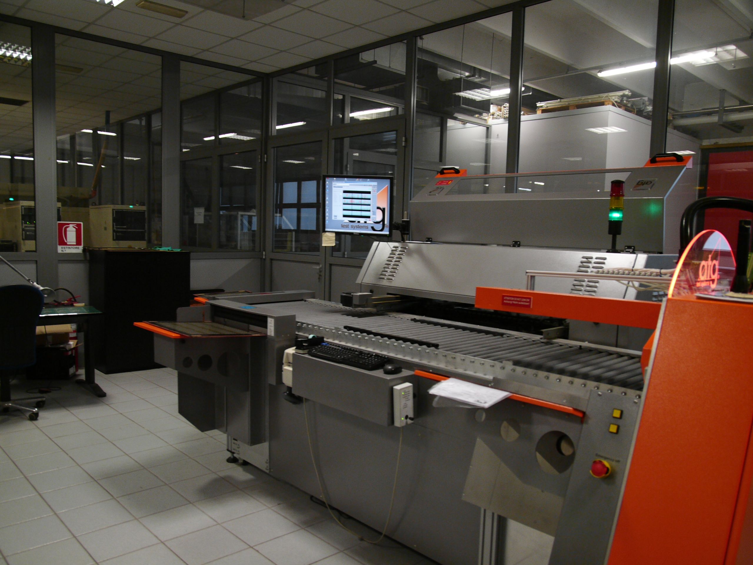
Finally, using a flying probe machine, an electrical test is performed to check for unexpected open circuits and shorts, the netlist file created during CAM is used.
Here we can see the USB Armory panel under final electrical testing on an ATG machine.
De-paneling, final inspection and shipping
Before being shipped out to the assembly factory, the assembly panels are cut from the working panel (12 assembly panels per working panel for the USB Armory). A final optical inspection is performed and the panels are vacuum-sealed and shipped to the assembly service.
Assembly
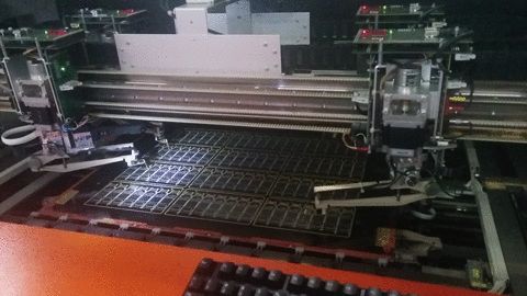
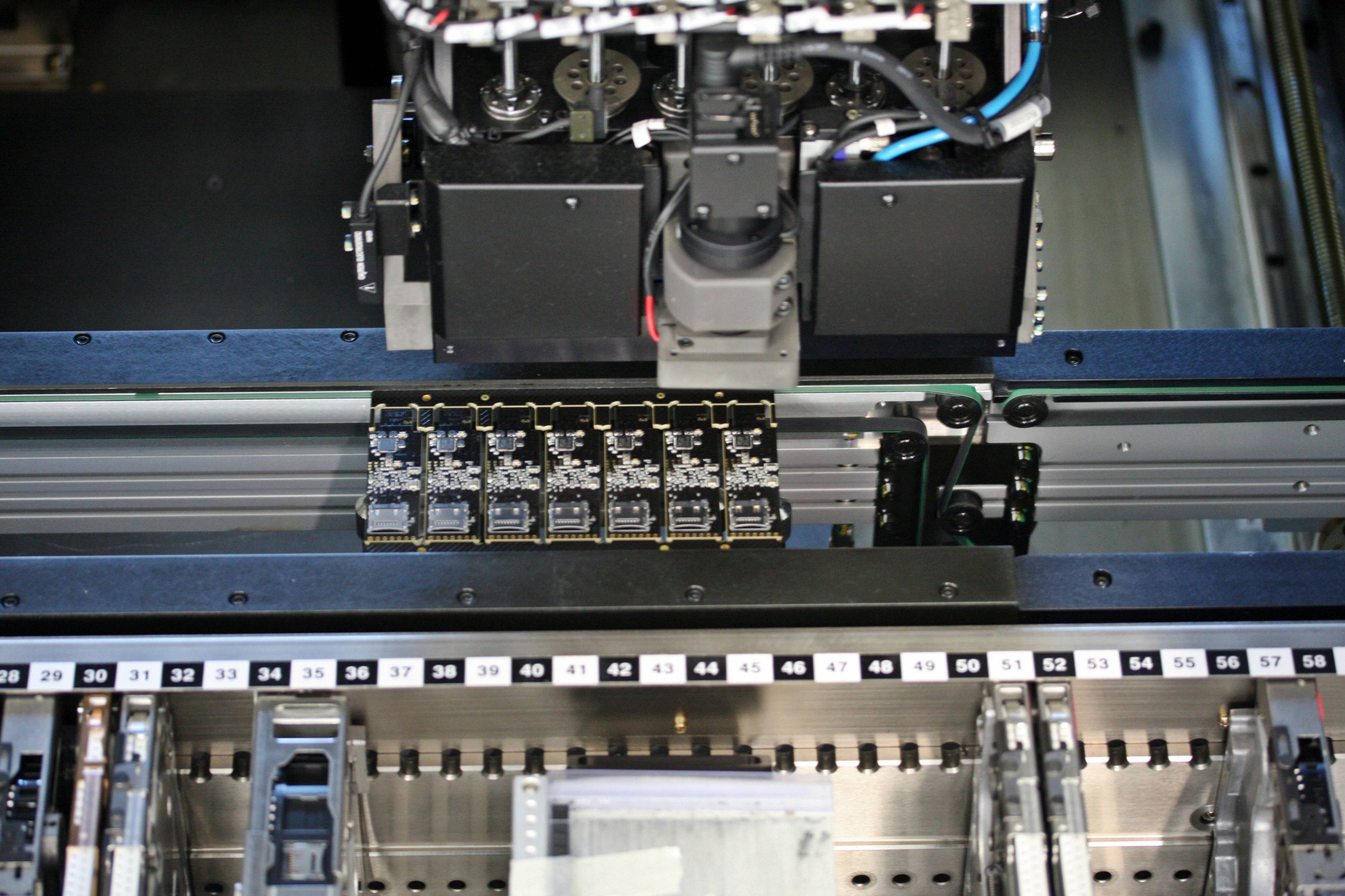
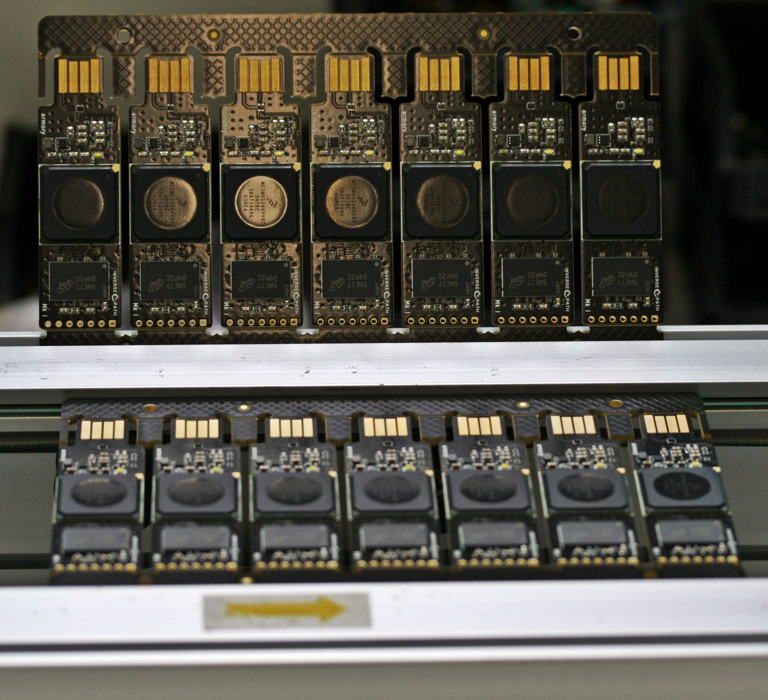
At the assembly factory the panels are individually inserted in the line pick-and-place machines (P&P), previously programmed and configured with the appropriate component reels.
The USB Armory has been assembled using Samsung SM 482 mounters and TSM reflow ovens.
X-ray inspection
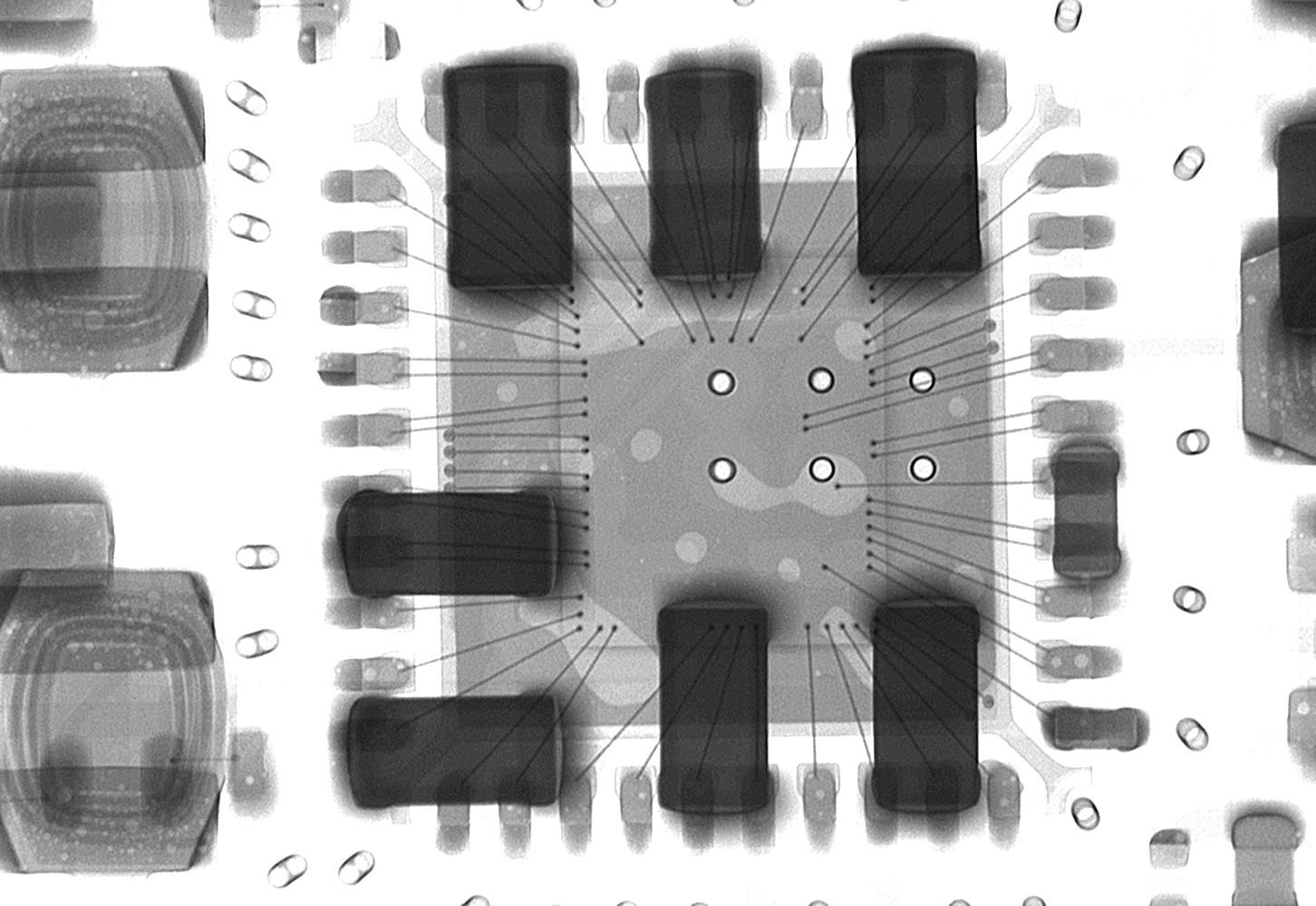
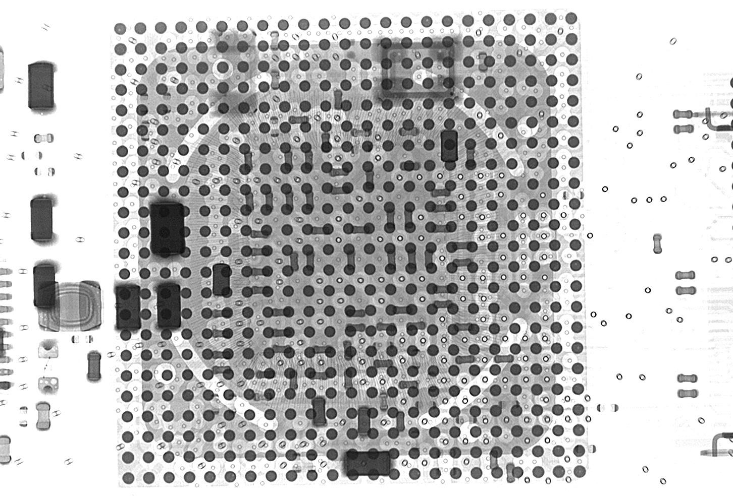
In the rare case of a faulty assembled board an x-ray inspection can help to determine where the flaw has been introduced.
Here we can see some beautiful shots of the USB Armory Power Management IC (PMIC):
The i.MX53 SoC:
And finally the entire board:


