Project update 3 of 5
Self-Destruct Design Experiments
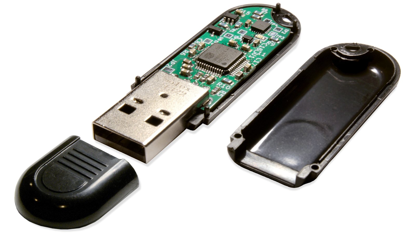
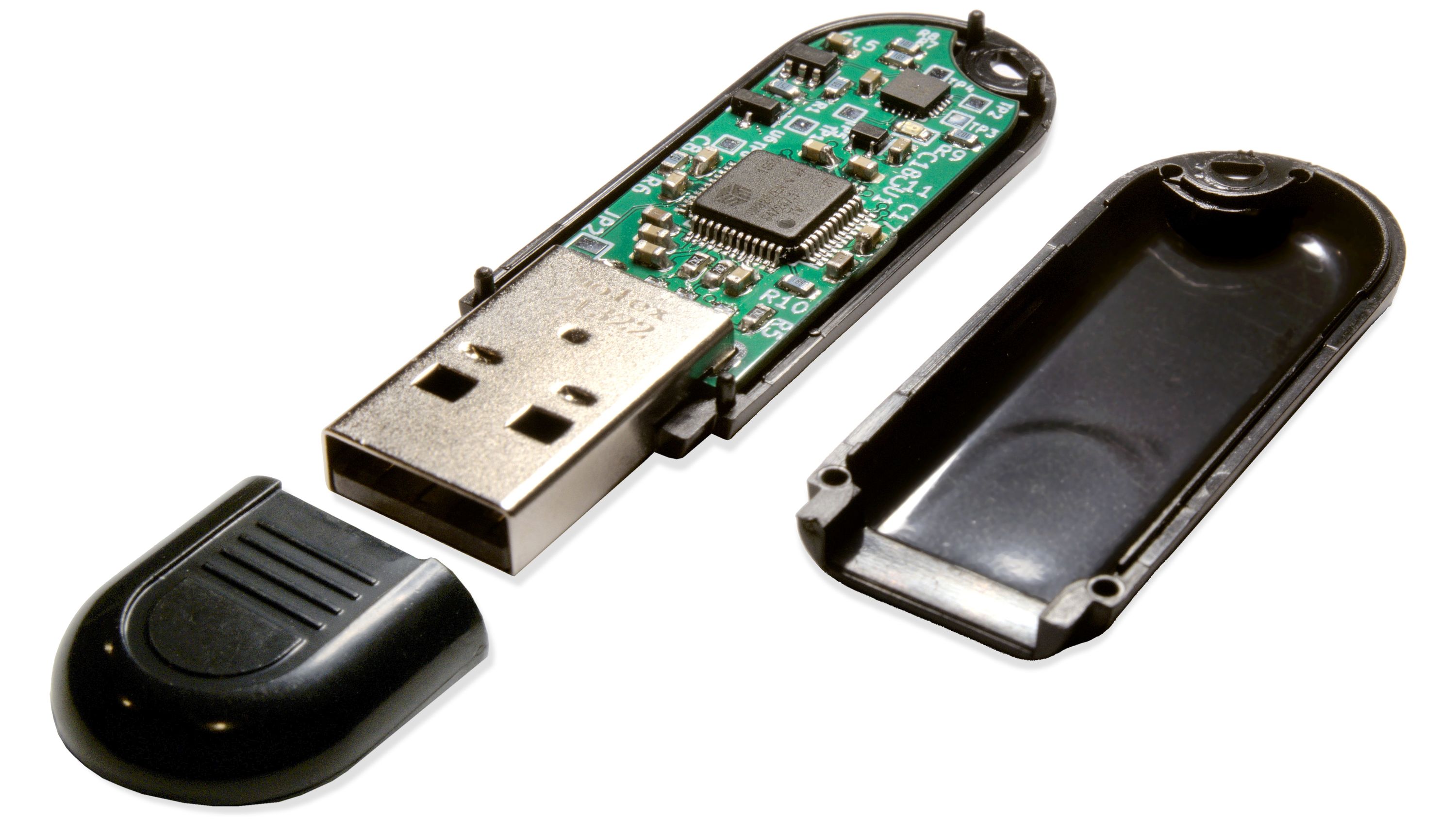
by Ryan WalkerOvrdrive USB is an open-hardware USB flash drive with an inconspicuous enclosure and a hidden security feature tucked away inside it. If you plug the device in normally, it will appear blank, but if you quickly plug it in three times in a row, you can read and write data. We built Ovrdrive for journalists working in hostile environments, security researchers, and anyone interested in open hardware.
We’re funded! Thanks so much to all the backers for bringing this project to life!
Ovrdrive is designed to be a discrete device; if the cops snatch a journalist in a non-privacy country, they shouldn’t think twice about a loose USB drive. When they plug it in, the device shouldn’t explode, melt, release corrosive material, or do anything else insane (even though that would make it a more exciting device). It should quietly destroy itself beyond repair. In this update, I’ll go over the path I took to get to the final destruction circuit and some of the issues I faced along the way.
Boost Circuit
My initial solution was to overload the flash memory voltage rail. This is the first time I’ve ever looked at the absolute maximum ratings of a component with the intent to go outside rather than stay within them.
The part needs to be pushed over 4.6V to be completely disabled. I can use a simple voltage doubler off the 5V line.
When Distruct_PWM is low, Ca will charge to 4.3V, which is 5V minus the 0.7V drop over the diode. When I set Distruct_PWM high from the MCU, the bottom of Ca is at 5V, giving a total potential of 9.3V. This flows into Cb and gets trapped for the next cycle. When you want to dump the energy into the flash IC, enable Q1 and say goodbye to those cute dog pics. This circuit worked once, but I had trouble getting it working consistently.
This circuit has a few issues. The first is energy storage; the amount of energy is proportional to the size of C2, and the more energy you have, the higher your probability of killing the flash. Our board space is limited and we can’t fit giant caps. The second issue is the Q1 NMOS. To turn on this FET, we need to boost its base voltage above the drain voltage. This isn’t impossible, but it requires some extra circuitry.
These two flaws and the inconsistency caused me to abandon this circuit.
H-Bridge
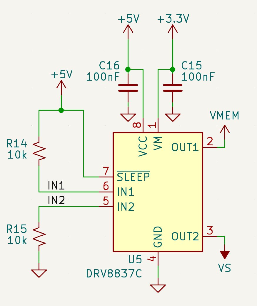
I asked around on Reddit to get some ideas on IC killing, and a very popular comment was, "Invert GND and Vcc; it has always killed my ICs." I settled on this, as it doesn’t suffer from the energy storage issue and is implementable through a standard H-bridge.
I won’t harp much on this because I wrote about it in the last update. But, here’s the circuit:
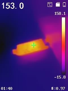
And here’s what happened:
I was excited to see things were working, but when I checked on the data, all the tests passed with flying colours. There seems to be a TVS diode or other reverse voltage protection inside the chip and the heat alone wasn’t enough to kill it.
H-Bridge + Overvoltage
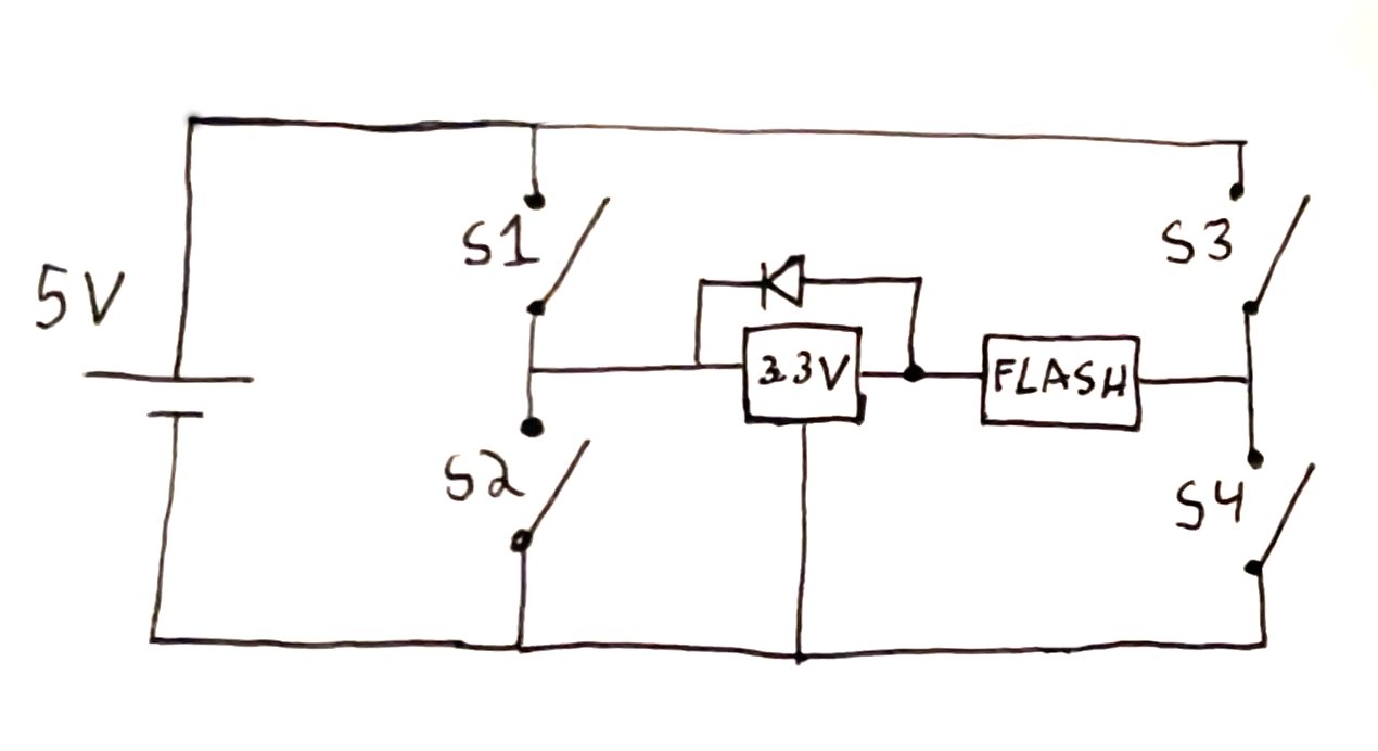
I then started looking into an overvoltage/reverse voltage combo.
When S1 and S4 are on, the chip receives its normal 3.3V for regular operation. When S2 and S3 are on, the chip will receive a reverse voltage of 5V. Even though the 3.3 regulator was working with this circuit, the flash didn’t work in normal operation. In destruction mode, the heating effect was similar to the previous method. I decided to abandon it.
Physical Methods
I started researching a few physical methods of destroying the flash. I found myself breaking up the sulpher on the tips of matches, looking into thermite, and I even discovered some ignitors that will probably get me put on a list somewhere.
These methods go against my core goal of the project, so I didn’t go much further, and at this time, I was getting a barrage of interest in a device to "hide its data". I left the H-bridge in to enable users to create their own thermally activated destruction methods, selling a USB that will "hide itself" by default!
Now here we are, fully funded! Thanks to you guys!
- Walker
