Project update 7 of 10
All The Latest Work-in-Progress
by Aleksa BHi all,
I’ve been juggling a lot of tasks lately, both for ThunderScope and otherwise. So this update is going to be a rundown of some work-in-progress stuff.
A Brief Rant About Schematics
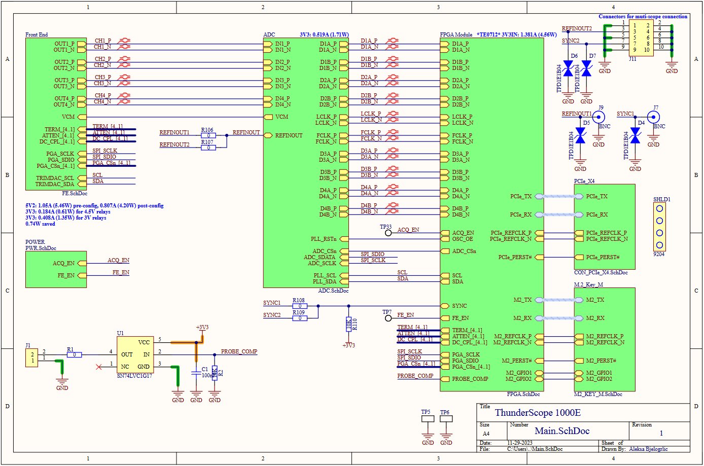
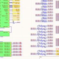
First of all, I overhauled the schematics for Rev. 5. To avoid making this update into a schematic design manifesto, I’ll focus only on the top level sheet here. This sheet hasn’t changed much since Rev. 1, so it felt great to really pick it apart and figure out why I wasn’t happy with it. Here’s the old top level sheet:
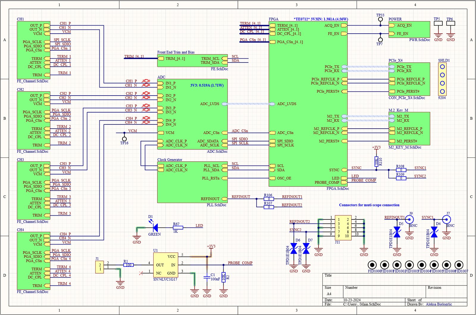
In a complex design like ThunderScope, the schematic can span many pages. A common tactic is to split each page into a block - this is called a “hierarchical” schematic. In hierarchical schematics, the top level page should function as a block diagram, allowing the reader to understand the system at a glance. Let’s take a look at the changes I’ve made to the Rev. 5 schematics and see if the top level sheet accomplishes this goal better than the old schematics.
There is only one block for the front end in the old schematics, so you would have to look at the net names on the signals to realize there are four channels. To make these inputs clearer, I have pulled them out of the front end block into four front end channel blocks. The remainder of the front end block got spun out into a front end trim and bias block, this also has the benefit of reducing the hierarchical depth of the block from two to one.
I like keeping the hierarchy as shallow as possible, so the reader can get the most information they can out of the top level sheet. I’ve pulled the clock generator out of the ADC block for the same reason (the only clue there was more going on in that block were the PLL signals!). I also made the ADC’s LVDS interface into a bus to declutter the blocks (no loss of meaning here, the bus does what it says on the tin).
The FPGA block gained another level of hierarchy since it has a bunch of stuff going on that would clutter up the top level sheet. This is a change from the old schematics since we are now putting the FPGA and associated components on the mainboard and not on a separate module.
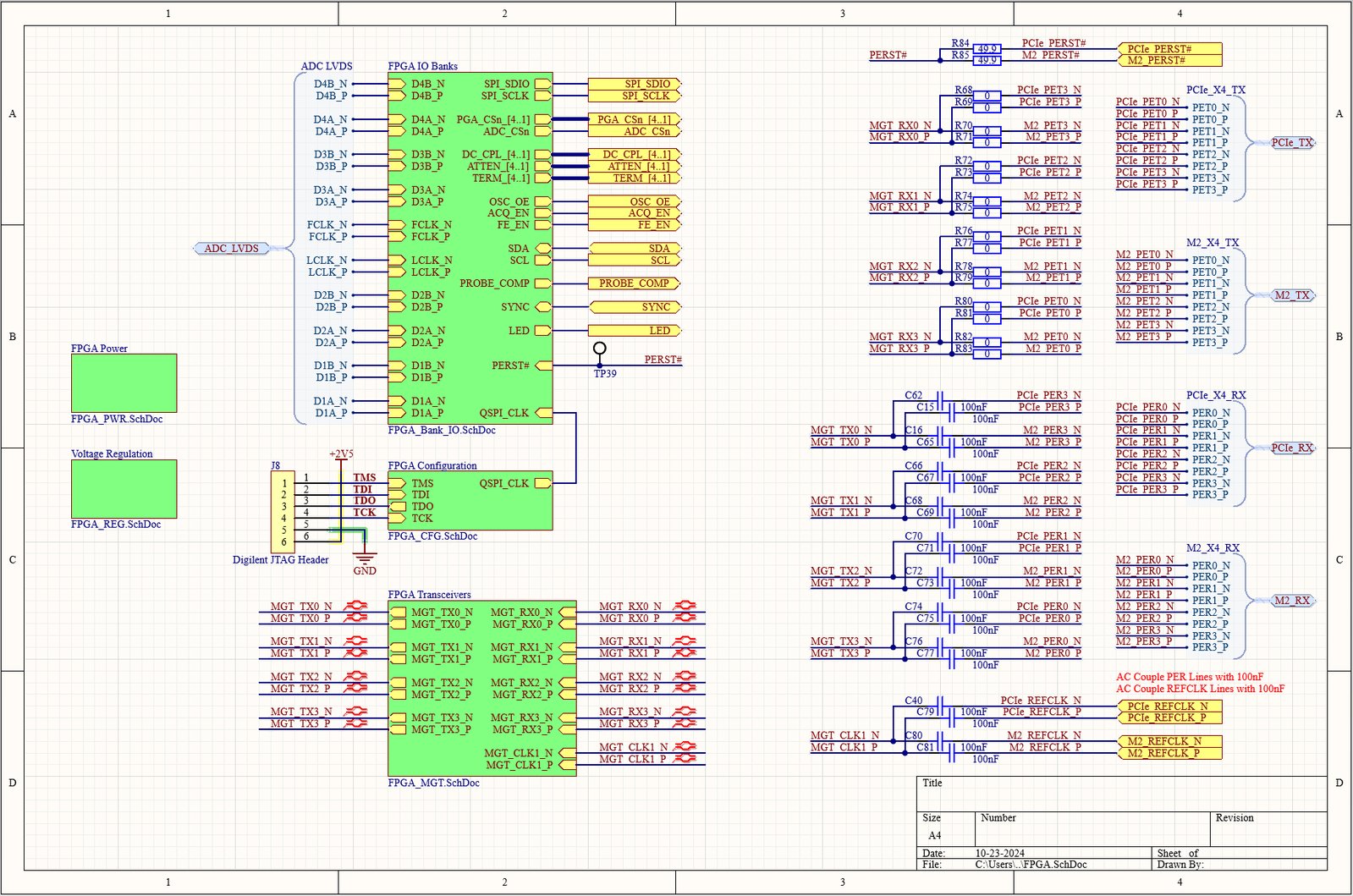
Ok, I said I’d only talk about the top level page, but actually it seems useful to talk about nested hierarchy for a bit. I treat the FPGA page much like the top page, trying to convey as much information as possible on how and why these blocks are connected this way. On the right you can see the stuffing options to choose PCIe or M.2 (used for Thunderbolt/USB4) connections, these are on the right side to match their location on the FPGA block on the top level sheet. These go into the transceiver block, and the LVDS bus and other IO go to the IO banks block. The config block takes a JTAG header input (it lives here since it’s not an interface the user should need to use in production and is therefore less pertinent to show on the top page), and finally there’s the FPGA power inputs and voltage regulation.
P.S. I know, I know, the default Altium colour scheme is gross and KiCad’s is much prettier (and open source). I’ll make the switch to KiCad after I deliver all the campaign units, I promise.
The Boards are Back in Town
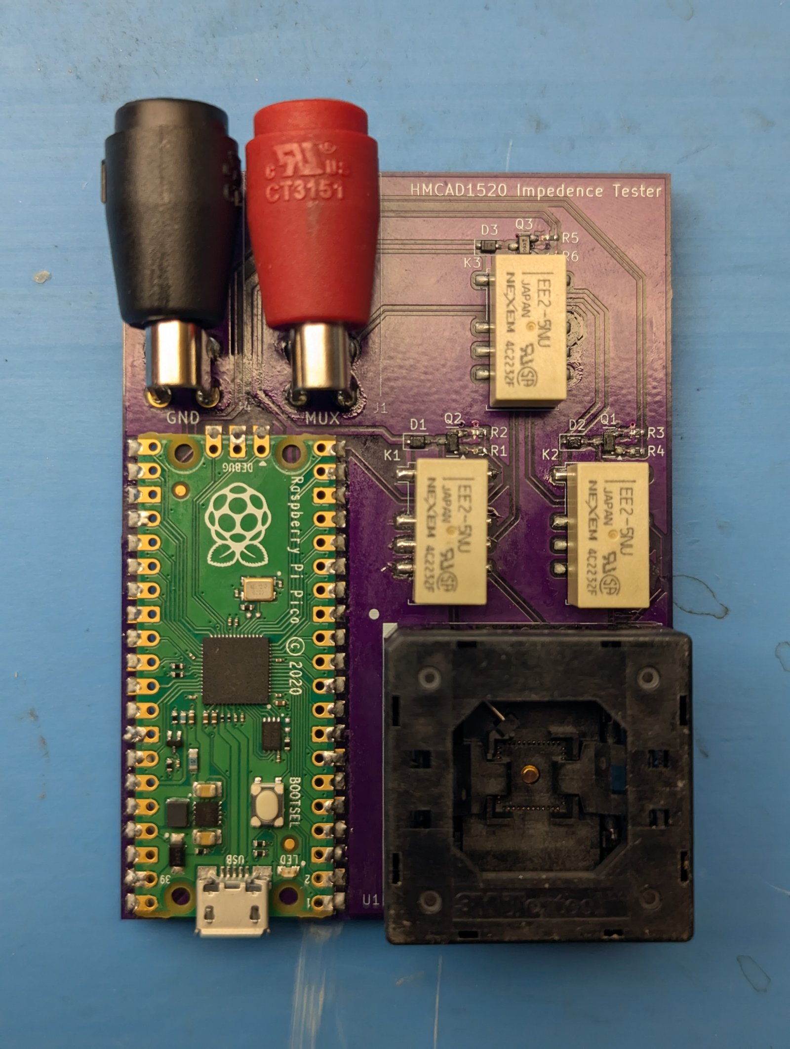
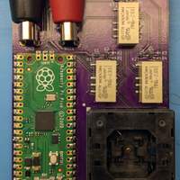
I mentioned I sent out a lot of boards in the first two updates, they came back from fab and I built them up. Here’s the HMCAD1520 impedance tester:
I’m going to write a test script for this board and start popping the ADCs into that small but mighty(-ly expensive) socket for testing soon.
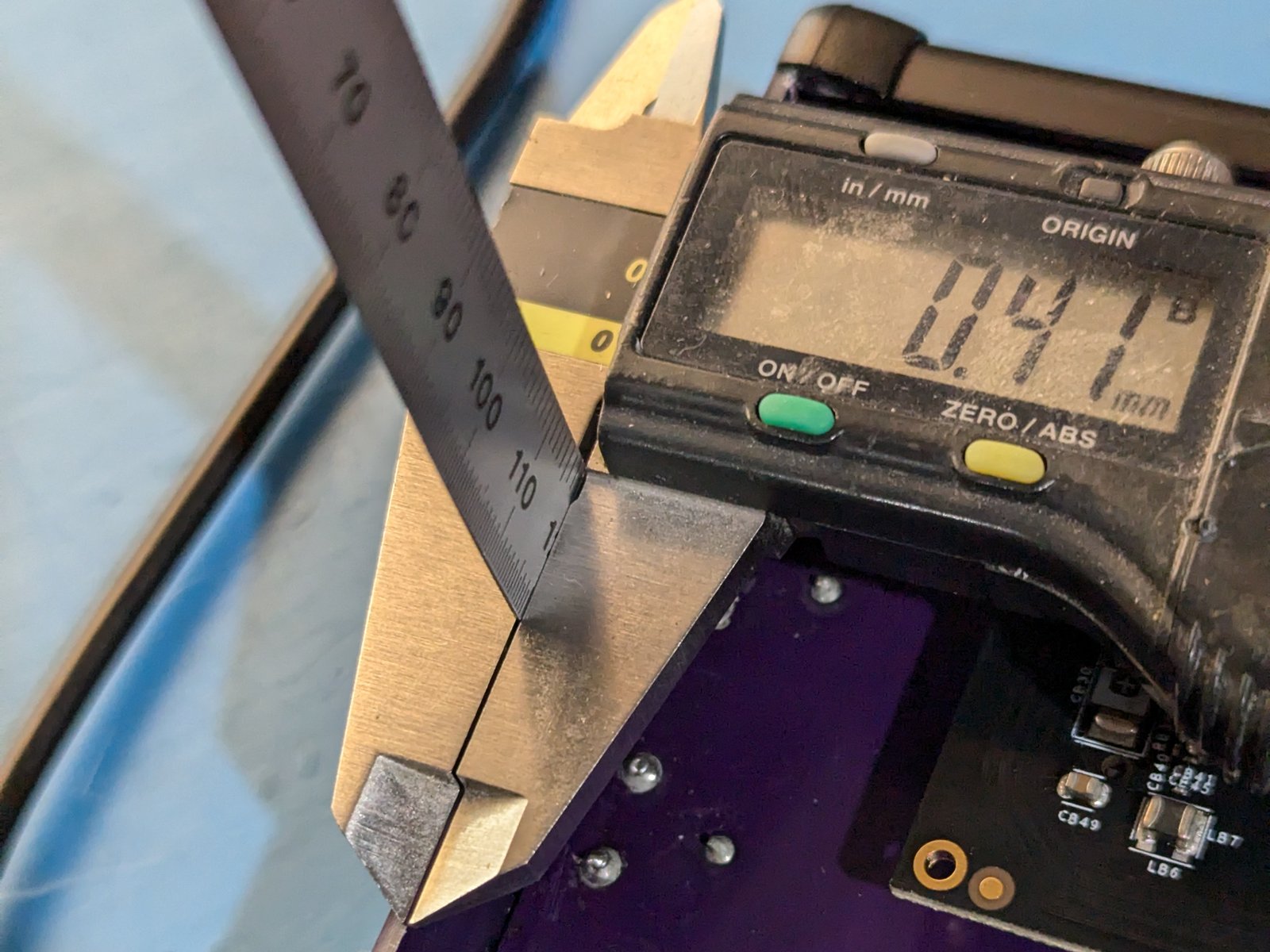
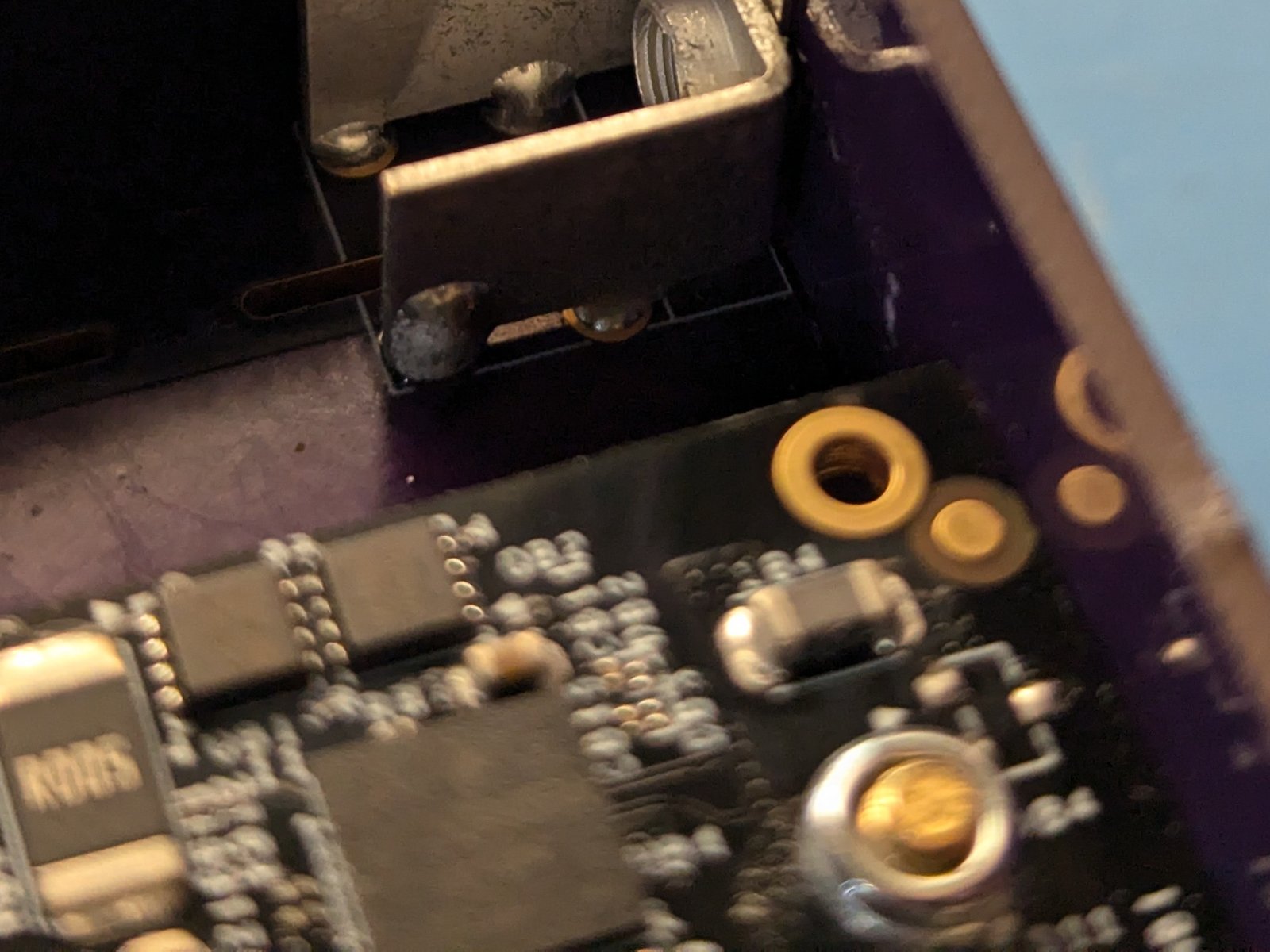
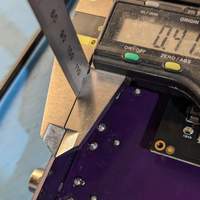
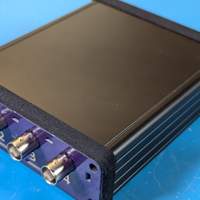
I also built up the mechanical model board and noted down all the fractions of millimeters that things need to move over by:
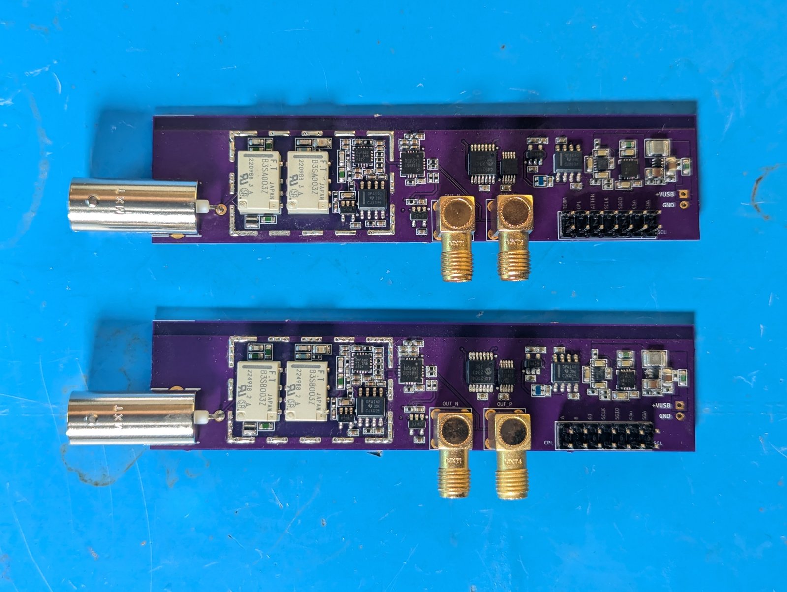
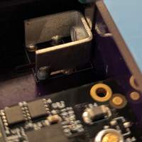
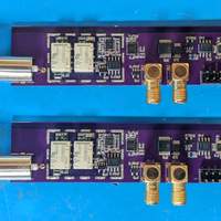
Two days under the microscope with tweezers and the front end test boards are finally assembled:
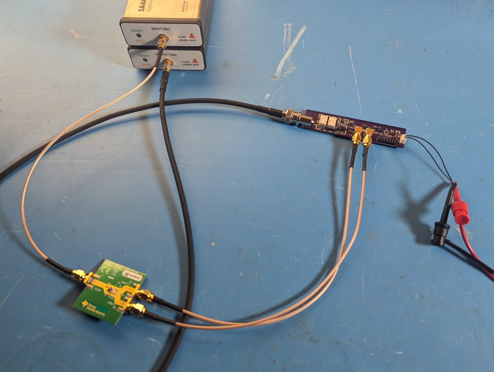
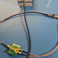
And I just started testing them now, results TBD:
From Powder to Goo: The Anti-Slip Saga Continues
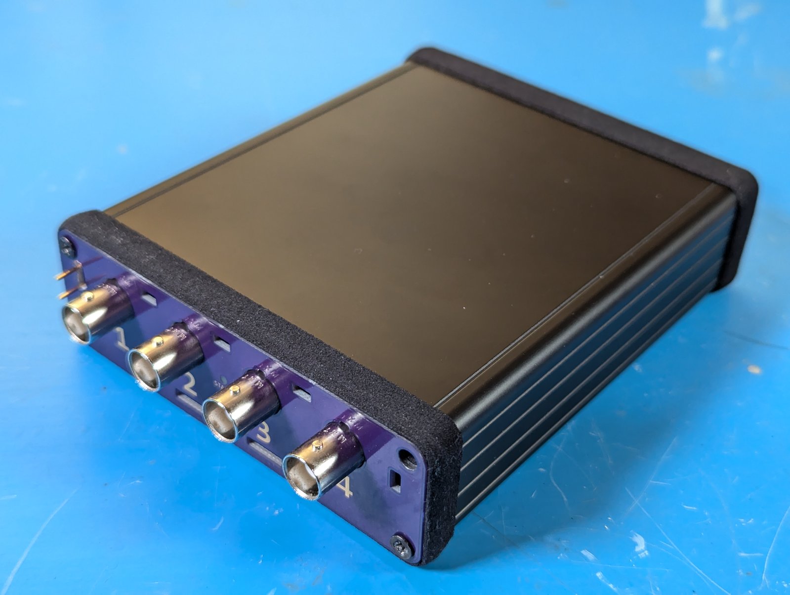
I received the anti-slip bumpers from a 3D printing service that did them in TPU using SLS 3D printing. Essentially, they used lasers to zap thermoplastic polyurethane powder together into a flexible, rubber-like finished product.
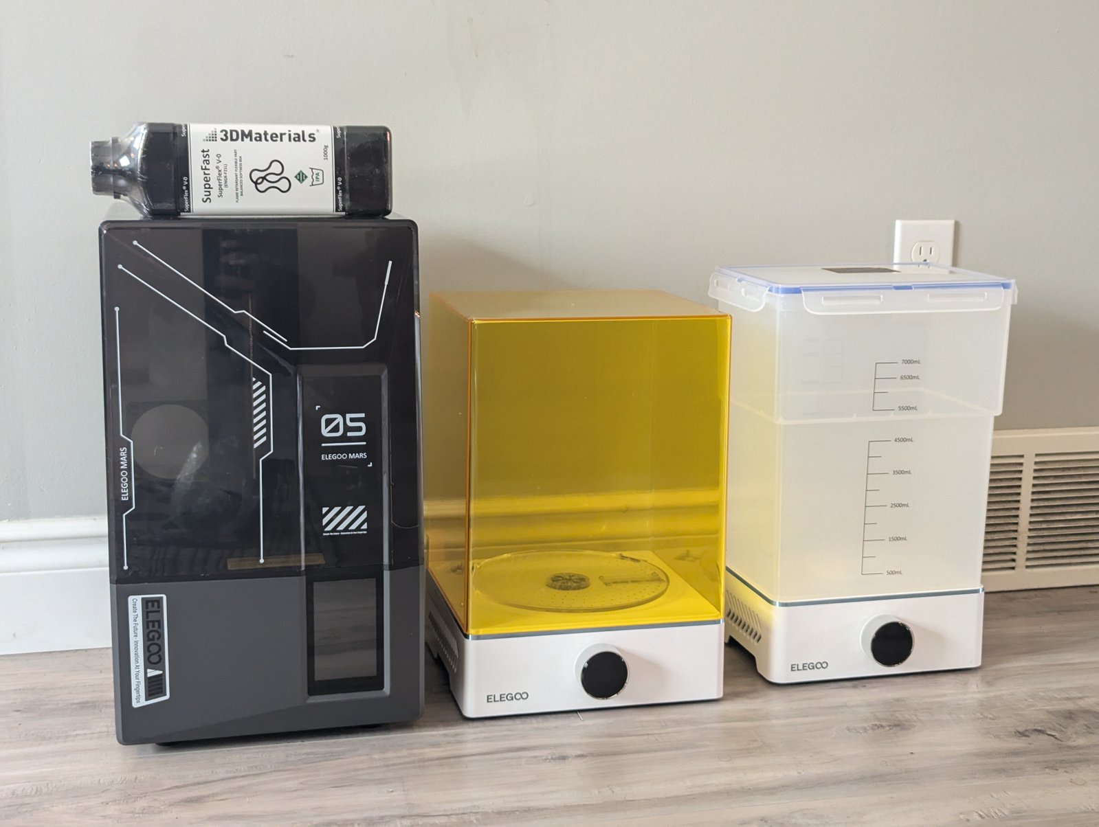
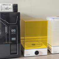
That surface texture though. So it does the job of stopping slippage, but at the cost of picking up every stray micron of dust it comes across. “I could do it better myself” I thought, mere seconds before buying an SLA printer.
Yes, the black resin feels very “World of Goo”, but that’s about where the fun ends. SLA printing uses moderately toxic UV-curable goo called "resin" which will irritate your skin and lungs without the proper PPE. I’ve kitted myself up and will be testing out various resins and mixes of resins until I find something I like.
And that’s about it from me, I should have the results of some of these tests and experiments for the next update, see ya’ll then!
-Aleksa
