Project update 7 of 8
First time right, QFP package details and test material
by Staf VAfter a good start the campaign is going slower now. We are over half way and 17% of the funding goal is reached. It is time now to back this project if you want it to succeed.
In this update I will discuss how first time right was taken as target for the Retro-uC project from the start; the details on the QFP package of the Retro-uC chip and the
First time right
A second source of comments on the Retro-uC campaign was about the fact the project assumes the chip will work the first time; in the industry also known as first-time-right. This goal has been taken into account during the definition of the Retro-uC project from the start. It was performed by applying the KISS principle at several levels of the project:
- re-use of well tested (open source) RTL as much as possible to avoid having bugs
- don't use analog blocks on the chips; they typically need one or more iterations to get right
- avoid feature creep by introducing lots of features that may also introduce bugs
- use of mature technology node; this reduces complexity of the chip and the maximum speed. This in itself will make is possible to have the timing, power distribution and signal integrity right from the first time.
A more detailed explanation can be found on a blog post on chips4makers.io
QFP package
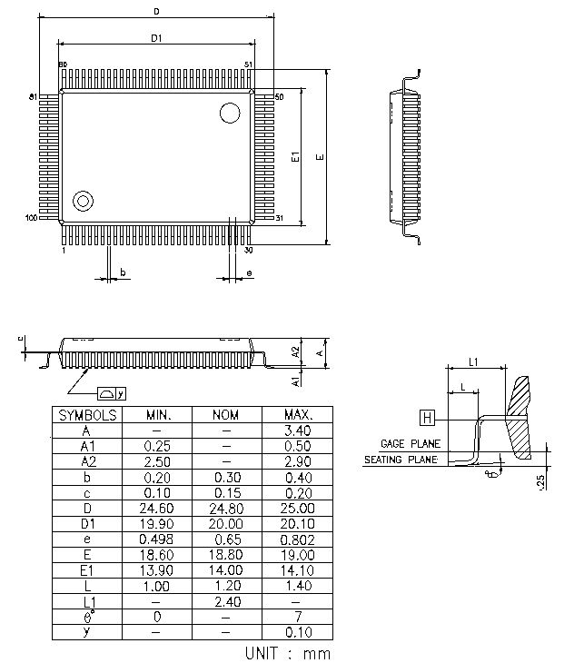
The package for the Retro-uC chip has been finalized. It will be a 100-pin QFP package of 14mm x 20mm. The details can be seen in the next picture:
You can see that this package is rectangular and has a 0.65mm pitch of the pins. A square version with a higher pin pitch was not available as open tool. Making a custom package would need more than $10 000 extra for the tooling start-up costs.
Also a preliminary pin list is given in the next table:
| Pin | Net |
|---|---|
| 1 | VCORE |
| 2 | GND |
| 3 | GND |
| 4 | VIO |
| 5-26 | PA1-PA22 |
| 27 | VIO |
| 28 | GND |
| 29 | GND |
| 30 | VCORE |
| 31-50 | PB1-PB20 |
| 51 | VCORE |
| 52 | GND |
| 53 | GND |
| 54 | VIO |
| 55-76 | PC1-PC22 |
| 77 | VIO |
| 78 | GND |
| 79 | GND |
| 80 | VCORE |
| 81-89 | PD1-PD9 |
| 90 | TDI |
| 91 | TDO |
| 92 | TCK |
| 93 | TMS |
| 94 | TRST_N |
| 95 | RESET_N |
| 96 | CLK |
| 97 | I2CBOOT |
| 98 | ENM68K |
| 99 | ENZ80 |
| 100 | EN6502 |
VCORE is the supply for the logic on the chip and has to be 3.3V; VIO can be chosen to be 3.3V or 5V to have 3.3V or 5V I/O. It still need to be finalized how the input and outputs of the peripherals are shared with the I/O pins on the chip. An update of the pin list will be given when this is done.
Development test material
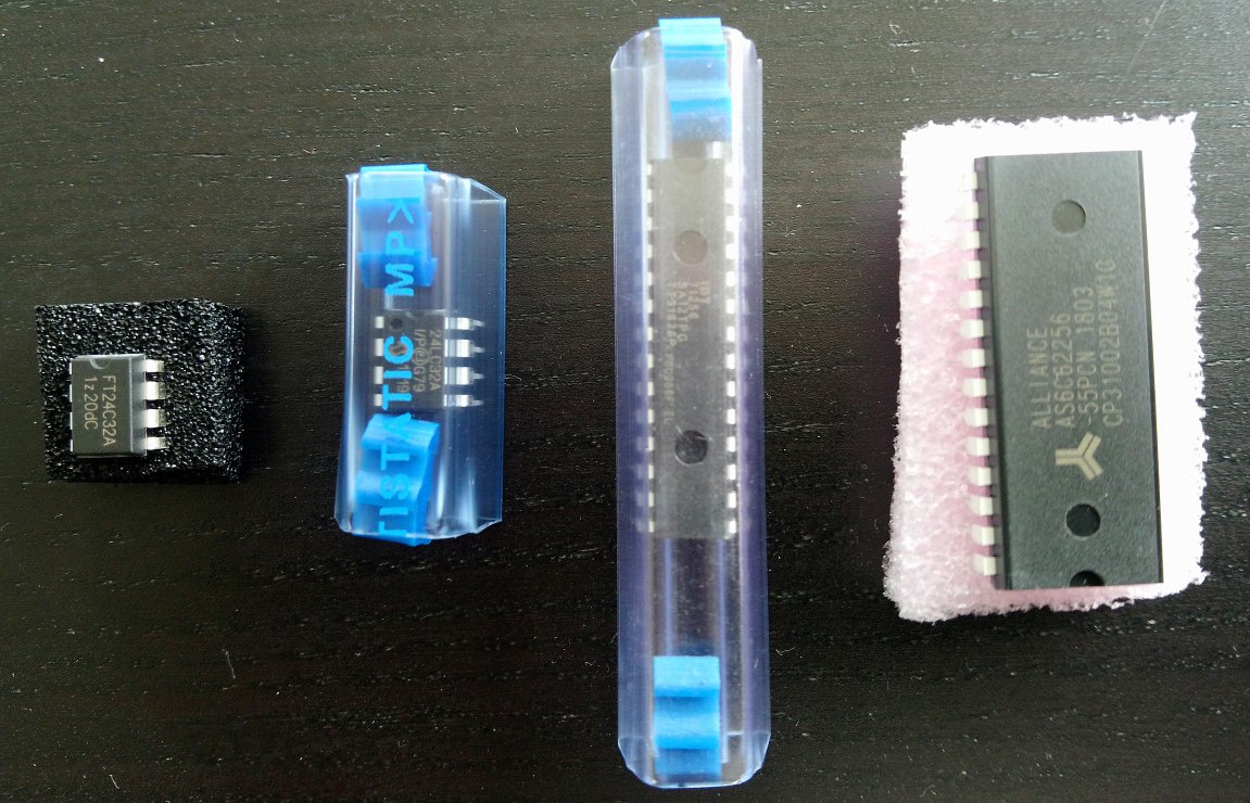
In order to test the peripherals on the Retro-uC I ordered some chips to allow testing the implementation on an FPGA. You can see the chips I got in the next picture:
You find the next chips on this photo (from left to right):
- Fremont Micro FT24C32A 32 kB I2C EEPROM
- Microchip 24LC32A 32kB I2C EEPROM
- IDT 71256SA 32 kB parallel SRAM
- Alliance Memory AS6C62256 32 kB parallel SRAM
These chips are meant to test the I2C boot feature of the Retro-uC and also for investigating the possibility of providing a SRAM interface on the pins of the Retro-uC. When successful it allows to have external memory extra to the 4 kB on chip memory or usable for other memory mapped access to external devices. This is a feature often requested that should allow to use the Retro-uC also as a microprocessor and not only as a microcontroller. I do think this feature should be able to be implemented without risk of messing up the rest of the chip so I am willing to make a compromise on the minimal number of features strategy to reach first time right for the Retro-uC. In one of the next updates it will be announced if this feature will be added to the Retro-uC.


