Project update 8 of 9
A Taste of Chip Design
As we work at full speed toward the May tapeout to qualify several blocks on 180 nm CMOS, we figured it would be a good time to pause just for a moment to give you a taste of what’s required to accomplish this kind of project. An open silicon system-on-chip (SoC) project has a lot of moving parts and minute details that all need to line up perfectly for it to function at all. Here are some of those details!
Some Design Constraints
We announced some time ago that we moved from a 130 nm mixed signal process to a 180 nm CMOS fully logic mask set. Although this move brought down the final budget, it brought us a lot of additional work to do, starting with porting operational circuitry in 130 nm to 180 nm. Traditional wisdom would imagine that porting analog circuitry would not be difficult when one scales up. However, the difficulty of the task is in the fact that the we have selected a vanilla logic 180 nm process without the mixed signal flavors to reduce mask costs. Usually, designing analog and RF circuitry requires additional mask layers that constitute passive devices, such as isolated capacitors, large resistors, varactors, vertical BJTs, and inductors with decent quality factors. Additional mask layers increase the mask set costs and therefore the chip cost in a low-to-medium production volume. Imagine yourself designing analog circuits without the freedom of having large isolated caps or large resistors without incurring in large area penalties. We are embracing this challenge and working on finishing the required peripherals to get an open silicon SoC in a low cost process.
Closed Versus Open
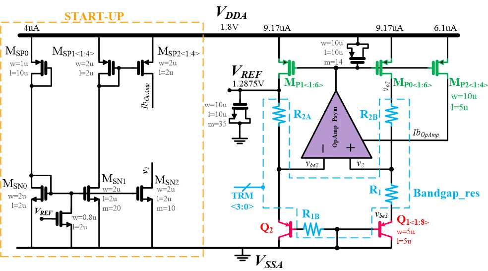
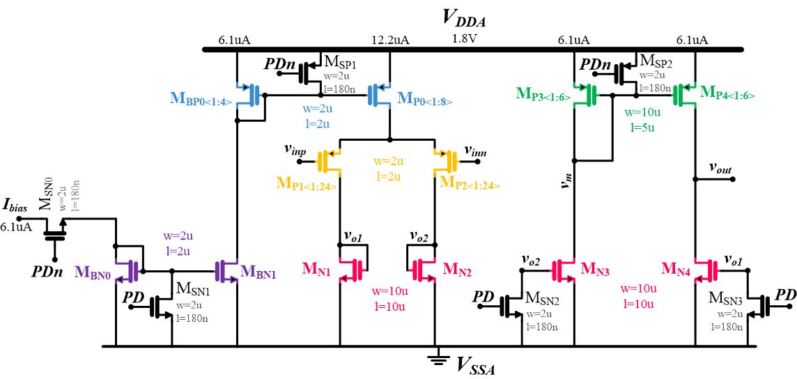
A typical MCU vendor would buy most of the IP blocks from a third party and then differentiate their design by adding some custom circuitry based on a customer requirement. Once the MCU has been sold to a particular customer, and depending of the contract terms, they will place the MCU in the store shelves looking for another killer app that allows them to generate further income gains. We decided to push the open silicon endeavour further, and we challenged ourselves by designing from scratch each of the required blocks to get an MCU working. To give you an idea, a silicon-proven voltage reference IP block might cost a project around $10k if you go and negotiate it at the IP market. In this update we would like to show you what it takes to get a "simple" voltage reference working by disclosing the real schematic of the bandgap being taped out inside the Open-V MCU.
Bandgap Voltage Reference
A voltage reference is an essential circuit in any chip. It is used for comparison, level detection, data conversion, biasing, etc. This reference should remain constant independent of external conditions like temperature, variations in the supply voltage, and process variations in fabrication, among others. The circuit shown in the figure above is one of the most widely used voltage references in the industry: a derivative of the Brokaw bandgap voltage reference (“bandgap” since the output voltage is close to the the theoretical 1.22 eV bandgap energy of silicon at 0°K).

Trimming the Voltage Reference
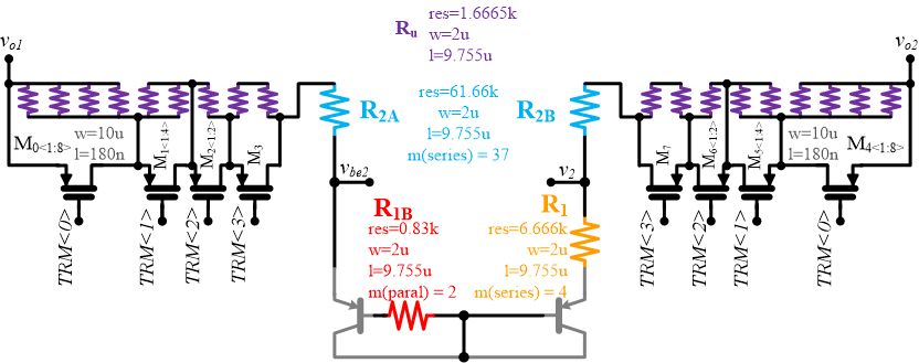
Because there is inevitably still some variation in the voltage reference between individual chips, it is standard practice to enable the chip to actually change the output voltage to a certain degree. This is called "trimming." The extent to which the chip can trim its reference voltage is determined by the number of bits dedicated to doing so. The exact method is shown in the diagram below.

In the Open-V, we have allocated four bits to trim the voltage reference using non-volatile registers. In an off-the-shelf SoC, the bandgap has been trimmed for you, which in certain applications might not be desirable. With the Open-V, you will get full documentation of how to do it, and better yet, circuit details of what is actually happening on-chip!
Simple Explanation of a Bandgap Reference
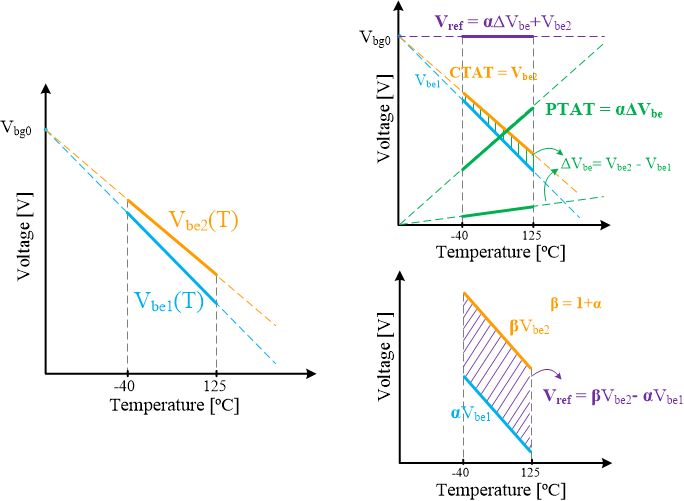
How does it work? One way to look at a bandgap voltage reference is that it is a circuit that linearly combines two or more (for higher order temperature compensation) base-emitter voltages, in order to cancel the temperature dependency of the output reference, as shown in the lower right plot below.

A More Complex Explanation
A bandgap voltage reference, in a first-order temperature analysis, is based on the linear combination of a PTAT (Proportional To Absolute Temperature) voltage and a CTAT (Complementary To Absolute Temperature) voltage. A base-emitter voltage (or emitter-base for a PNP BJT) has a CTAT behavior (Vbe1, Vbe2) as shown in the leftmost plot in the above diagram, while the subtraction of two different base-emitter voltages has a PTAT behavior (Delta{Vbe} = Vbe2-Vbe1). Referring to our bandgap voltage reference, the PTAT behavior is obtained from a current through the R1 resistor, which is then mirrored and multiplied by R2A to obtain the desired PTAT voltage (alpha = R2A/R1). The voltage reference is then obtained as the sum of the base-emitter voltage of Q2 (Vbe2) plus the PTAT voltage over R2B, as indicated in the upper right plot of the figure above.
Simulation Results
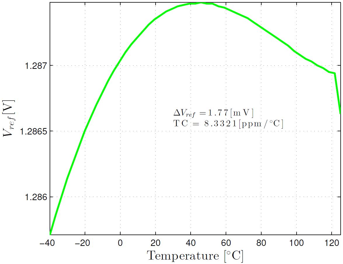
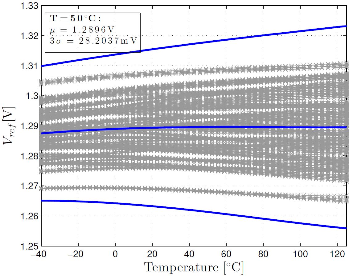
Monte Carlo simulations of the voltage reference output at typical and corner process variations are shown in the two plots below. Note that we verified performance for 3-sigma in order to get a high yield. The 3-sigma variation for 73 simulation corners with respective Monte Carlo runs is 28 mV without trimming.


