Spread over various videos, writings, and mailing list discussions, a picture is beginning to emerge of a suitable microarchitecture.
There are several things to remember about this design, the primary being that it is not explicitly intended as a discrete GPU (although one could be made). Instead, it is primarily for a battery-operated, power-efficient hand-held device, where it happens to just about pass on, say, a low to mid-range Chromebook. Power consumption for the entire chip is targeted at 2.5 watts.
We learned quite quickly that, paradoxically, even a mobile embedded 3D GPU requires an extreme number of registers (128 floating-point registers) because it is handling vectors (or quads as they are called), and even pixel data, in floating-point format, which means four 32-bit numbers (including the transparency). So, where a "normal" RISC processor has 32 registers, a GPU typically has to have four times that many simply because it is dealing with four lots of numbers simultaneously. If you don’t do this, then that data has to go back down to memory (even to L1 cache), and, as the L1 cache runs a CAM, it’s guaranteed to be power-hungry.
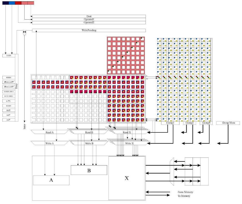
Dealing with 128 registers brings some unique challenges not normally faced by general purpose CPUs, and when it becomes possible (or a requirement) to access even down to the byte level of those 64-bit registers as "elements" in a vector operation, it is even more challenging. Recall Mitch Alsup’s scoreboard dependency floor plan (reproduced with kind permission, here):
There are two key dependency matrices here: on the left is the function unit (rows) to register file (columns), where you can see at the bottom in the CDC 6600 the register file is divided down into A, B and X. On the right is the function unit to function unit dependency matrix, which ensures that each function unit only starts its arithmetic operations when its dependent function units have created the results it needs. Thus, that matrix expresses source register to destination register dependencies.
Now, let’s do something hair-raising. Let’s do two crazed things at once: increase the number of registers to a whopping 256 total (128 floating point and 128 integer), and at the same time allow those 64-bit registers to be broken down into eight separate 8-bit values… and allow function unit dependencies to exist on them!
If we didn’t properly take this into account in the design, then an 8-bit ADD would require us to "lock", say, Register R5 (all 64 bits of it), absolutely preventing and prohibiting the other seven bytes of R5 from being used, until such time as that extremely small 8-bit ADD had completed. Such a design would be laughed at, its performance would be so low. Only one 8-bit ADD per clock cycle, when Intel has recently added 512-bit SIMD?
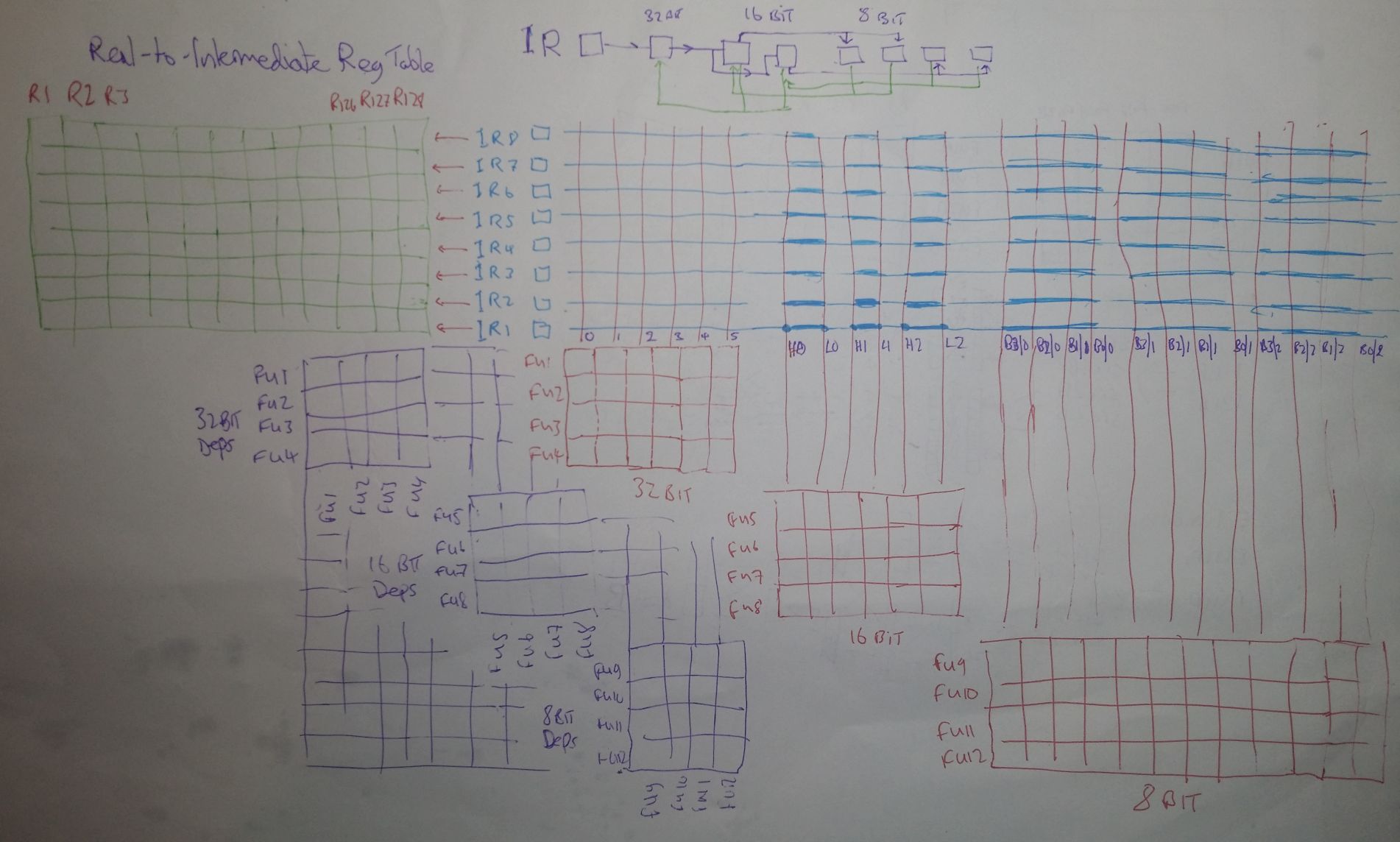
Here’s a proposed solution. What if, when an 8-bit operation needs to do a calculation to go into the first byte, the other seven bytes have their own completely separate dependency lines in the register and function unit matrices? It looks like this:
If you recall from the previous updates about scoreboards, it’s not the "scoreboard" that’s the key, it’s these register to function unit and function unit to function unit dependency matrices that are the misunderstood key. Let’s explain the above diagram. Firstly, in purple in the bottom left, is a massive matrix of function units to function units, just as with the standard CDC 6600, except now there are separate 32-bit function units, 16-bit function units, and 8-bit function units. In this way, we can have a 32-bit ADD depending on and waiting for an 8-bit computation, or a 16-bit MUL on a 32-bit SQRT and so on. Nothing obviously different there.
Likewise, in the bottom right, in red, we see matrices that have function units along rows, and registers along the columns, exactly again as with the CDC 6600 standard scoreboard. However, again, we note that because there are separate 32-bit function units and separate 16-bit and 8-bit function units, there are three separate sets of function unit to register matrices. Also, note that these are separate, where they would be expected to be grouped together. Except, they’re not independent, and that’s where the diagram at the top (middle) comes in.
The diagram at the top says, in words, "if you need a 32-bit register for an operation (using a 32-bit function unit), the 16-bit and 8-bit function units also connected to that exact same register must be prevented from occurring. Also, if you need eight bits of a register, whilst it does not prevent the other bytes of the register from being used, it does prevent the overlapping 16-bit portion and the 32-bit and the 64-bit portions of that same named register from being used."
This "cascading" relationship is absolutely essential to understand. If you need register R1 (all of it), you cannot go and allocate any of that register for use in any 32-bit, 16-bit, or 8-bit operations. This is common sense! However, if you use the lowest byte (byte 1), you can still use the top three 16-bit portions of R1, and you can also still use byte 2. This is also common sense!
So in fact, it’s actually quite simple, and this "cascade" is simply and easily propagated down to the function unit dependency matrices, stopping 32-bit operations from overwriting 8-bit and vice-versa.
Virtual Registers
The fourth part of the above diagram is the grid in green, in the top left corner. This is a "virtual" to "real" one-bit table. It’s here because the size of these matrices is so enormous that there is deep concern about the line driver strength, as well as the actual size. 128 registers means that one single gate, when it goes high or low, has to "drive" the input of 128 other gates. That takes longer and longer to do, the higher the number of gates, so it becomes a critical factor in determining the maximum speed of the entire processor. We will have to keep an eye on this.
So, to keep the function unit to register matrix size down, this "virtual" register concept was introduced. Only one bit in each row of the green table may be active: it says, for example, "IR1 actually represents that there is an instruction being executed using R3." This does mean, however, that if this table is not high enough (not enough IRs), the processor has to stall until an instruction is completed, so that one register becomes free. Again, another thing to keep an eye on, in simulations.
Refinements
The second major concern is the purple matrix, the function unit to function unit one. Basically, where previously we would have FU1 cover all ADDs, FU2 would cover all MUL operations, FU3 covers BRANCH, and so on, now we have to multiply those numbers by four (64-bit ops, 32-bit ops, 16-bit, and 8), which in turn means that the size of the FU-to-FU matrix has gone up by a staggering sixteen times. This is not really acceptable, so we have to do something different.
The refinement is based on an observation that 16-bit operations of course may be constructed from 8-bit values, and that 64-bit operations can be constructed from 32-bit ones. So, what if we skipped the cascade on 64 and 16 bit, and made the cascade out of just 32-bit and 8-bit? Then, very simply, the top half of a 64-bit source register is allocated to one function unit, the bottom half to the one next to it, and when it comes to actually passing the source registers to the relevant ALU, take from both function units.
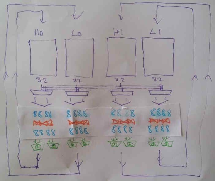
For 3D, the primary focus is on 32-bit (single-precision floating-point) performance anyway, so if 64-bit operations happen to have half the number of reservation stations / function units, and block more often, we actually don’t mind so much. Also, we can still apply the same "banks" trick on the register file, except this time with four-way multiplexing on 32-bit wide banks, and 4 x 4 crossbars on the bytes as well:
To cope with 16-bit operations, pairs of 8-bit values in adjacent function units are reserved. Likewise for 64-bit operations, the 8-bit crossbars are not used, and pairs of 32-bit source values in adjacent Function Units in the 32-bit function unit area are reserved.
However, the gate count in such a staggered crossbar arrangement is insane: bear in mind that this will be 3R1W or 2R1W (2 or 3 reads, 1 write per register), and that means three sets of crossbars, comprising four banks, with effectively 16 byte to 16 byte routing.
It’s too much - so in later updates, this will be explored further.


