Project update 3 of 9
Prototyping the USB Insight Hub
by David SIn this update, I want to share the prototyping process I followed for the USB Insight Hub. Materializing an idea requires various hardware iterations, which are evidence of the trials, errors and fixes that lead to a production-worthy product. So here is a brief exposé for those curious, like me, about the unglamorous work behind the scenes.
The First Prototype
Initially I just wanted to test the viability of the idea, something “simple” that would allow me to answer the following questions:
- Can you extract port enumerators?
- Which screen is most fit for the best display experience?
- What is the best way to measure voltage and current?
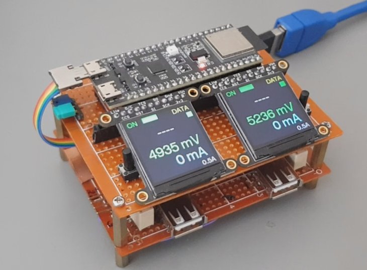
I searched through the elements I already had: a microcontroller (ESP32-S3-DevKitM-1) and a voltage and current meter (based on ATTINY3226), all mounted with a generic USB Hub 2.0 that I had abandoned. For the screens, I acquired a couple of displays (Adafruit 1.3" 240x240 Wide Angle TFT LCD Display) and some electronic switches (AP22653AW6). Later on, I added two low signal relays to interrupt the USB data signal.
I carried out the assembly using two breadboards, and the following ugly but functional prototype was born:
Moving to PCB
This first prototype gave me many of the answers I needed: it was possible to extract the enumerators with a relatively simple program developed in C#, the size and resolution of the screen I chose were correct (smaller would prevent correct viewing from an appropriate distance) and, although the ATTINY3226 ADC is extremely versatile, it came with limitations in terms of accuracy and stability, requiring an external reference and calibration procedure.
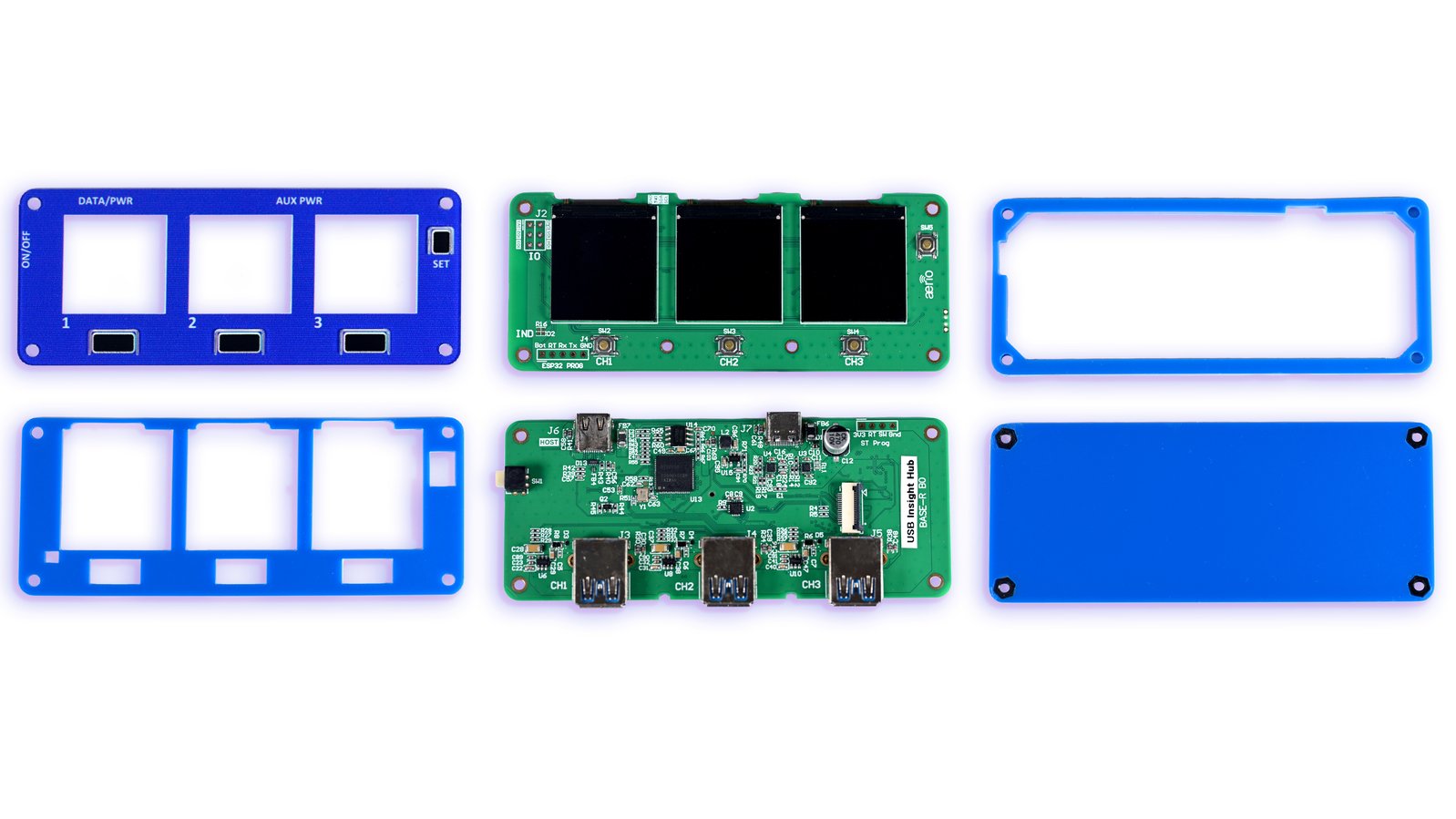
From here I started a design directly on PCB since this allowed me to integrate parts with footprints that were very difficult to mount on a breadboard. This leap was huge, not only because the design was made to include a Renesas uPD720210 Hub 3.0 chip (and all the associated differential routing for USB signals), a power muxer, and a Microchip PAC1943 current meter, but also the mechanical design had to be made so that USB Insight Hub would have good usability and practicality for eventual production.
The first PCB prototype (A0) was soldered and ready to test; those who have been through this process will understand the satisfaction of knowing that it turns on, nothing is shorted, and you get the awaited prize: finding more than 50 changes necessary between errors and improvements.
Assembly Process
From previous projects, I knew that the assembly and soldering of components had to be done locally. Logistics in Ecuador (where I am located) are cumbersome and that adds a lot of time between development cycles. For boards that have components only on one side, a hot plate is generally a good option. However, in my case, the design required populating both sides of the PCB, so I used a homemade oven with an electronic relay and a Raspberry Pi Zero W running the PicoReflow program as the oven controller. Please enjoy some photos of the process used to manually assemble the PCB with components on both sides:
Current Iteration
The next PCB iteration (B0) incorporated the corrections from A0 and has been used in the last four months and throughout the Crowd Supply campaign process. Is this the last iteration? Surely not. I’ve found some small details that still need working but, above all, I’ll need to work with the PCBA contractor so that the board is suitable for manufacturing (DFM) on an SMD assembly line.
Thanks for the support so far from all the backers and, to anyone, please don´t hesitate to Ask a Question via our Crowd Supply campaign page, where you can also back our campaign if you haven’t already!
Cheers,
David


